
A sharp uptick in reported counterfeit and nonconforming electronic components in 2024 has underscored a widening threat to component authenticity, according to the latest ERAI Annual Report.
Continue reading

A sharp uptick in reported counterfeit and nonconforming electronic components in 2024 has underscored a widening threat to component authenticity, according to the latest ERAI Annual Report.
Continue reading
Scientists at Tianjin University, China, have developed a pioneering nondestructive testing technology for micro-LED wafers, offering a much-needed solution to a long-standing industry challenge through a novel “soft-touch” approach.
Continue reading
Researchers from UConn and the U.S. Naval Research Laboratory have outlined new ways to accurately track and manage heat in ultrawide bandgap semiconductors, a challenge that has become increasingly important as these materials drive the future of high-performance electronics.
Continue reading
Scientists at the University of Tennessee, Knoxville, recently discovered that Mn3Si2Te6 changes from an insulator to an electrically conductive metal when exposed to a magnetic field.
Continue reading
Master Bond Inc., Hackensack, N.J., released its newest product, Master Bond EP29LPSPND-3, a two component, non-drip epoxy compound with a paste consistency that can be used for bonding and sealing applications.
Continue reading
Researchers at the Korea Research Institute of Standards and Science have developed a real-time diagnostic system for semiconductor plasma process parts which is expected to enhance yield, stability, and cost efficiency by preemptively preventing contaminant particles generated from component corrosion.
Continue reading
Researchers at Stanford Engineering have developed an ultrathin material that conducts electricity better than copper and could enable more energy-efficient nanoelectronics.
Continue reading
The Department of Energy has announced funding $179 million for three Microelectronics Science Research Centers that bring together multi-institutional, multidisciplinary projects in partnership with industry organized around making microelectronics more energy efficient and able to operate better in extreme environments.
Continue reading
Researchers at Iowa State University, Ames, Iowa, have successfully demonstrated a groundbreaking zero-gravity 3D printing technology using electrohydrodynamic printing and nanoink, paving the way for on-demand manufacturing and electronics repair in space.
Continue reading
Researchers at the University of Minnesota have achieved a new artificially designed material that allows electrons to move faster while remaining transparent to both visible and ultraviolet light, breaking the previous record and being pivotal in making the next generation of high-power electronics faster, transparent and more efficient.
Continue reading
Researchers at University of Pennsylvania demonstrated memory technology capable of enduring temperatures as high as 600° Celsius—more than twice the tolerance of any commercial drives on the market—and these characteristics were maintained for more than 60 hours, indicating exceptional stability and reliability.
Continue reading
Scientists at Lawrence Berkeley National Laboratory, Berkeley, Calif., developed microcapacitors with ultrahigh energy and power density, paving the way for on-chip energy storage in electronic devices.
Continue reading
Researchers at the University of Surrey, England, University of Cambridge, the Chinese Academy of Sciences, Xidian University, and Zhengzhou University, China, built a new kind of two-faced (bifacial) solar panel using single-walled carbon nanotubes as both front and back electrodes that are the highest efficiency single junction solar cells to date.
Continue reading
The Center for Harsh Environment Semiconductors and Systems is the first initiative of the university’s North Texas Semiconductor Institute.
Continue reading
Researchers at North Carolina State University, Raleigh, N.C., have created a robot called RoboMapper that can rapidly identify new perovskite materials with improved stability and solar cell efficiency and is capable of conducting experiments more efficiently and sustainably to develop a range of new semiconductor materials with desirable attributes.
Continue reading
Magnetoelectric material is first of its kind able to directly stimulate neural tissue
Continue reading
Developed by researchers from Lawrence Berkeley National Laboratory (Berkeley Lab) and UC Berkeley, a new semiconducting material called “multielement ink” is the first “high-entropy” semiconductor that can be processed at low or room temperature, making the semiconductor purification and development process significantly less heat-intensive and more sustainable.
Continue reading
Researchers at the University of Illinois Urbana-Champaign have developed a semiconductor device made using diamond, that has the highest breakdown voltage and lowest leakage current compared to previously reported diamond devices.
Continue reading
An international team, including researchers from Washington University in St. Louis, Massachusetts Institute of Technology, Yonsei University and Inha University in Korea, Georgia Institute of Technology, and the University of Notre Dame, has demonstrated the monolithic 3D integration of layered 2D material into novel processing hardware, addressing the challenge of increased information transfer time between functional components in advanced computer chips and paving the way for AI computing.
Continue reading
Onsemi, Scottsdale, Ariz., opened an application test lab in Piestany, Slovakia, focused on the advancement of system solutions for battery/plug-in hybrid/electric vehicles and energy infrastructure power conversion systems.
Continue reading
Weebit Nano Limited, Israel, a leading developer of advanced memory technologies for the global semiconductor industry, and SkyWater Technology, Bloomington, Minn., the trusted technology realization partner, announced that Weebit’s Resistive Random-Access Memory IP module has been fully qualified in SkyWater’s 130nm CMOS process at temperatures of up to 125 degrees Celsius – the temperature specified for Grade-1 automotive applications.
Continue reading
Materials scientist Frank Mücklich, Professor of Functional Materials at Saarland University, Germany, has developed a laser surface texturing procedure that makes the surfaces of electrical contacts more stable and more efficient.
Continue reading
Johns Hopkins Applied Physics Laboratory (APL) researchers have developed one of the world’s smallest, most intense and fastest refrigeration devices, the wearable thin-film thermoelectric cooler (TFTEC), and teamed with neuroscientists to help amputees perceive a sense of temperature with their phantom limbs.
Continue readingRigaku, Japan, leading provider of X-ray metrology solutions for semiconductor in-line processes, research and development, and high-volume manufacturing, has opened its first Semiconductor Metrology Technology Center in Sunnyvale, CA.
Continue readingAn international research group with researchers from China, Japan, and the Los Alamos National Laboratory, Los Alamos, NM, developed a new surface coating technology that is capable of significantly increasing electron emission in materials.
Continue readingIn a new study, Lam Research Corp., Fremont, Calif., examined the potential for the use of artificial intelligence in process development for chip fabrication and found that a “human first, computer last” approach can reach process engineering targets dramatically faster and at half the cost compared to today’s approach.
Continue reading A study at the University of Rochester, Rochester, N.Y., suggests perovskites — a family of materials nicknamed for their crystalline structure that have shown extraordinary promise in recent years as a far less expensive, equally efficient replacement for silicon in solar cells and detectors — may become far more efficient.
Researchers typically synthesize perovskites in a wet lab, and then apply the material as a film on a glass substrate and explore various applications. Chunlei Guo, professor of optics at the University of Rochester leading the study reported in Nature Photonics, instead proposes a novel, physics-based approach.
By using a substrate of either a layer of metal or alternating layers of metal and dielectric material—rather than glass—he and his coauthors found they could increase the perovskite’s light conversion efficiency by 250 percent.
“No one else has come to this observation in perovskites,” Guo says. “All of a sudden, we can put a metal platform under a perovskite, utterly changing the interaction of the electrons within the perovskite. Thus, we use a physical method to engineer that interaction.”
Metals are probably the simplest materials in nature, but they can be made to acquire complex functions. The Guo Lab has extensive experience in this direction. The lab has pioneered a range of technologies transforming simple metals to pitch black, superhydrophilic (water-attracting), or superhydrophobic (water-repellent). The enhanced metals have been used for solar energy absorption and water purification in their recent studies.
In this new paper, instead of presenting a way to enhance the metal itself, the Guo Lab demonstrates how to use the metal to enhance the efficiency of pervoskites.
“A piece of metal can do just as much work as complex chemical engineering in a wet lab,” says Guo, adding that the new research may be particularly useful for future solar energy harvesting.”
In a solar cell, photons from sunlight need to interact with and excite electrons, causing the electrons to leave their atomic cores and generating an electrical current, Guo explains. Ideally, the solar cell would use materials that are weak to pull the excited electrons back to the atomic cores and stop the electrical current.
Guo’s lab demonstrated that such recombination could be substantially prevented by combining a perovskite material with either a layer of metal or a metamaterial substrate consisting of alternating layers of silver, a noble metal, and aluminum oxide, a dielectric.
The result was a significant reduction of electron recombination through “a lot of surprising physics,” Guo says. In effect, the metal layer serves as a mirror, which creates reversed images of electron-hole pairs, weakening the ability of the electrons to recombine with the holes.
The lab was able to use a simple detector to observe the resulting 250 percent increase in efficiency of light conversion.
Several challenges must be resolved before perovskites become practical for applications, especially their tendency to degrade relatively quickly. Currently, researchers are racing to find new, more stable perovskite materials.
“As new perovskites emerge, we can then use our physics-based method to further enhance their performance,” Guo says.
Image – This illustration from the Guo Lab shows the interaction between a perovskite material (cyan) and a substrate of metal-dielectric material. The red and blue pairings are electron-hole pairs. Mirror images reflected from the substrate reduce the ability of excited electrons in the perovskite to recombine with their atomic cores, increasing the efficiency of the perovskite to harvest solar light. Courtesy of: Chloe Zhang.
For more information:
University of Rochester
 Veeco Instruments Inc., Plainview, NY, acquired Epiluvac AB, Sweden, a privately held manufacturer of chemical vapor deposition (CVD) epitaxy systems that enable advanced silicon carbide (SiC) applications in the electric vehicle market. Epiluvac’s technology platform combined with Veeco’s global go-to-market capabilities create a significant long-term growth driver for Veeco.
The desire for clean, efficient, and reduced fossil-fuel energy is driving tremendous growth in the electric vehicle market. Applications such as on-board charging, fast charging and powertrain inverters are ideally suited for SiC power devices. The SiC device market is forecasted to grow approximately 30% compound annual growth rate (CAGR) from 2023 through 2027 according to Yole Group. Accordingly, the SiC epitaxy equipment market is expected to grow approximately 15% CAGR over the same time period according to Yole Group and internal Veeco estimates.
“The Epiluvac team has developed a superior platform and process know-how aligned with markets that are a great strategic fit for Veeco,” said Bill Miller, Veeco’s Chief Executive Officer. “Their well-designed CVD platform achieves high productivity, is easy to maintain and has superior process control capability that make it uniquely qualified to produce devices that enable lighter, smaller and more efficient power conversion systems. We see this acquisition as a great complement to our metal organic chemical vapor deposition epitaxy product line. This acquisition accelerates our penetration into the emerging, high-growth SiC equipment market by reducing our time to market.”
“We are excited to join Veeco, a recognized leader in semiconductor and compound semiconductor capital equipment,” commented Per-Anders Eriksson, Epiluvac’s chief executive officer. “Our complementary technology platforms, along with Veeco’s extensive worldwide sales, service and manufacturing capabilities, will position us well to help our customers enable accelerated SiC adoption. The decades of research and development the Epiluvac team has invested in this demanding epitaxial process will be a great asset to Veeco’s already impressive process capabilities.”
Epiluvac is an early-stage revenue company with 11 employees. The purchase price for the transaction, all payable in cash, is $30 million paid at the time of closing with a potential additional $35 million in performance based earn-outs. The impact to Veeco’s financial results are not expected to be material in 2023 and volume revenue is expected to begin in 2024.
For more information:
Epiluvac AB
Veeco
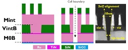 Imec, Belgium, a world-leading research and innovation hub in nanoelectronics and digital technologies, presents a semi-damascene integration approach for implementing the vertical-horizontal-vertical (VHV) scaling booster – intended to enable 4-track (4T) standard cells. The semi-damascene process enables cell boundary scaling down to 8nm tip-to-tip (T2T) in the middle-of-line (MOL) layers, providing self-aligned edges.
This provides a booster that designers can use for packing standard cells tighter, representing a 21 percent area gain over 5T designs. The novel routing scheme, along with the semi-damascene integration approach, will be critical to gradually push the logic scaling roadmap well into the Å era.
For a long time, the MOL, which provides the connection between the front-end-of-line (FEOL) and back-end-of-line (BEOL), has been organized as a single-layer contact. But currently, it is expanding into several layers, including, for example, the Mint and Vint layers. These MOL layers carry the electrical signals from the transistor’s source, drain, and gate to the local interconnects and vice versa.
Imec recently introduced a novel standard cell routing architecture called VHV, which involves the introduction of an extra MOL layer (M0B) as a scaling booster to enable 4T standard cell designs. With this booster, the first three routing layers in the standard cell follow a VHV routing style instead of the traditional HVH routing style in 5T standard cells. However, the novel two-level MOL VHV scaling booster is challenging from a process integration point of view, mainly arising from the tight boundary between neighboring 4T standard cells. The cell boundary requires a tight T2T between adjacent MOL M0B lines and two vias (VintB) facing each other with well-defined via edges – all at a minimum distance of one critical dimension (CD) of the top Mint layer. This means that the T2T and VintB via distance will need to be gradually reduced from ~24nm to ~8nm for upcoming technology nodes. This can no longer be achieved using a direct lithographic print but requires a self-aligned patterning strategy instead.
Researchers defined the tight boundary between adjacent standard cells using a two-level semi-damascene approach involving a direct metal etch. Zsolt Tőkei, program director of nano-interconnects and fellow at imec said, “Roughly speaking, we start from conventionally defined continuous lines and wider vias and, once two metal layers are finished, we split them into two, using the top 16-18nm pitch Mint layer as a hard mask for the final patterning step. This results in 3 edges (of Mint, VintB, and M0B) that are simultaneously self-aligned. With our Ru-based two-level test vehicle, we obtained an average via CD of 10.5nm and M0B T2T as tight as 8.9nm – a key achievement.” Imec researchers complemented structural validation with an initial electrical characterization of line resistance and isolation properties.
“The VHV routing scheme is a critical scaling booster to enable cell boundaries at the A10, A7, A5, A3 technology nodes,” adds Tőkei. “It also applies to future device architectures such as nanosheet, forksheet, and CFET. By extending semi-damascene from the BEOL towards the MOL, we have now also found a way to integrate this promising booster. More detailed investigations will, however, be needed, and for that purpose, imec is taping out a new dedicated mask.”
Image – (Left/middle) Schematic representation of the semi-damascene process flow used to test the key features of VHV. (Right) TEM image of the test vehicle after the final Ru etch: T2T M0B and VintB via are self-aligned to the 18mn pitch Mint layer.
For more information:
Imec
 Researchers in Drexel University’s College of Engineering have developed a thin film device fabricated by spray coating that can block electromagnetic radiation with the flip of a switch. The breakthrough, enabled by versatile two-dimensional materials called MXenes, could adjust the performance of electronic devices, strengthen wireless connections, and secure mobile communications against intrusion.
The team previously demonstrated that two-dimensional layered MXene materials – discovered just over a decade ago – when combined with an electrolyte solution, can be turned into a potent active shield against electromagnetic waves. This latest MXene discovery, reported in Nature Nanotechnology, shows how this shielding can be tuned when a small voltage – less than that produced by an alkaline battery – is applied.
MXene is a unique material in that it is highly conductive making it perfectly suited for reflecting microwave radiation that could cause static, feedback, or diminish the performance of communications devices. But its internal chemical structure can also be temporarily altered to allow these electromagnetic waves to pass through.
This means that a thin coating on a device or electrical components prevents them from both emitting electromagnetic waves, as well as being penetrated by those emitted by other electronics. Eliminating the possibility of interference from both internal and external sources can ensure the performance of the device, but some waves must be allowed to exit and enter when it is being used for communication.
The key to eliciting bidirectional tunability of MXene’s shielding property is using the flow and expulsion of ions to alternately expand and compress the space between material’s layers, like an accordion, as well as to change the surface chemistry of MXenes.
With a small voltage applied to the film, ions enter – or intercalate – between the MXene layers altering the charge of their surface and inducing electrostatic attraction, which serves to change the layer spacing, the conductivity and shielding efficiency of the material. When the ions are deintercalated as the current is switched off, the MXene layers return to their original state.
The team tested 10 different MXene-electrolyte combinations, applying each via paint sprayer in a layer about 30 to 100 times thinner than a human hair. The materials consistently demonstrated the dynamic tunability of shielding efficiency in blocking microwave radiation, which is impossible for traditional metals like copper and steel. And the device sustained the performance through more than 500 charge-discharge cycles.
These results indicate that the MXene films can convert from electromagnetic interference shielding to quasi-electromagnetic wave transmission by electrochemical oxidation of MXenes. The MXene film can potentially serve as a dynamic EMI shielding switch.
For security applications, the team suggests that the MXene shielding could hide devices from detection by radar or other tracing systems. The team also tested the potential of a one-way shielding switch. This would allow a device to remain undetectable and protected from unauthorized access until it is deployed for use.
The next step for the team is to explore additional MXene-electrolyte combinations and mechanisms to fine-tune the shielding to achieve a stronger modulation of electromagnetic wave transmission and dynamic adjustment to block radiation at a variety of bandwidths.
For more information:
Drexel University