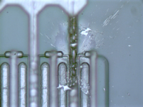
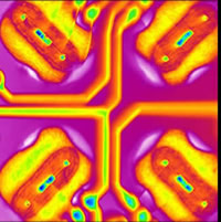
Incoming! This RF device suffered severe electrical overstress at the metal drain finger, resulting in this 3 dimensional “explosion” effect! Has this event ended, or is it still ongoing?
2nd Place:
Mark Lam Tiam Weng
Institute of Microelectronics, Singapore
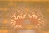
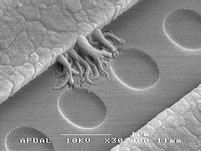
Particle on top of wafer with Low K
Dielectric Film. The Flame like
defect looks like the chinese character
“Huo” for fire.
3rd Place:
Ray Haythornthwaite
Semiconductor Insights, Canada
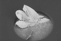
Image of an “exploding” failed Light Emitting Diode (LED).
Category II: Black and White Images
1st Place:
Murali Hanabe, Sesil Mathew, and Sridhar Canumalla
Nokia, Texas
A SnAgCu solder ball in a chip scale package (CSP) was etched away to reveal non-wetted areas on the Cu pad on the CSP. The picture shows the growth of Ag3Sn intermetallic phase with dendritic morphology from the Cu6Sn5 scallop-shaped intermetallic phase on the Cu pad. The Cu6Sn5 intermetallic also forms hexagonal, rod-shaped crystals. The non-wetted areas were contributing to early failure by acting as crack initiation sites.
2nd Place:
Jay Kopycinski
Freescale, Arizona
SEM image of ESD induced overstress
damage at gate poly of MOS transistor.
Fused polysilicon can be seen stretching
from the gate poly (left) to the source
contact area.
3rd Place:
Brett Engel and John Petrus
IBM, New York
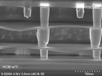
3-Dimentional SEM image depicting thermal cycle induced shear in an isolated stacked via structure in copper interconnect
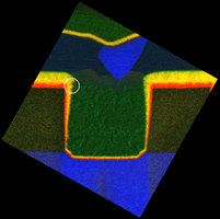
EFTEM color image of a cross-section through an Al metal line and W “plug” contact. In this image, Si is blue, Ti is red, and TiN is yellow. A Si-rich nodule is visible, as well as a potential failure site in the TiN barrier that could result in “volcano” formation.
2nd Place:
Olivier Crepel, Solomon Woods and Lee Knauss
Crepel – Philips, France
Woods and Knauss – Neocera, Maryland
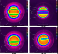
Magnetic field distribution of an
RF Inductor measured with a
magnetoresistive sensor.
3rd Place:
Otwin Breitenstein
Max Planck Institute of Microstructure Physics, Germany
Lock-in thermogram of an integrated circuit after ESD stressing (T-modulation amplitude image, Tmax = 10 mK). The bright spots are sites of leakage currents, the weakest ones dissipating about 100 microwatts.