As electronic devices evolve to include more functionality in smaller form factors, advanced packaging—integrating multiple semiconductor components into a compact 3D structure—has become essential. This growing complexity, particularly in technologies like high-bandwidth memory (HBM), poses significant challenges for quality control. Traditional 2D X-ray radiography often falls short when it comes to identifying sub-micron defects in critical interconnects such as micro-bumps and through-silicon vias (TSVs).
To address this, researchers at Dragonfly, a brand of Comet Group, Switzerland, explored applying high-resolution 3D X-ray imaging to inspect HBM stacks at unprecedented detail. They evaluated 20 µm micro-bumps in an HBM stack, where sub-micron voids and cracks can critically affect performance and yield.
The workflow began with a rapid 30-second nano-CT overview scan at 2.6 µm voxel size, which provided a full-field visualization of the HBM sample. Despite the quick acquisition, the image quality was sufficient to for an overview investigation of the HBM micro-bumps such as alignment and missing bumps for example. This also served as a guide for selecting regions of interest (ROIs) for detailed analysis.
A subsequent high-resolution scan at 600 nm voxel size took approximately 75 minutes, enabled the clear resolution of structural features such as cracks and voids within individual micro-bumps and TSVs.
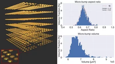
Dragonfly 3D World advanced visualization software platform performed extensive 3D segmentation and quantitative analysis of the high-resolution datasets. In total, 1275 micro-bumps and 1680 voids were identified and characterized by parameters including volume, aspect ratio, sphericity, and radii. The statistical results highlighted shape anomalies that may indicate defective joints. Most voids were small and spherical but the detection of larger and elongated voids could point to potential risks for reliability.
3D World enables early detection of potential failure modes, supports process optimization, and helps improve overall yield in advanced packaging.
This study demonstrates that 3D X-ray techniques, particularly nano-CT, are powerful tools for the rapid, high-resolution inspection of modern electronic packaging. As interconnect dimensions continue to shrink and integration becomes more complex, non-destructive 3D imaging will play an increasingly vital role in ensuring device reliability and accelerating innovation.
Image – Overview of micro bumps from Dragonfly 3D World with voids identified and bump bond statistics.
For more information:
Dragonfly
https://dragonfly.comet.tech