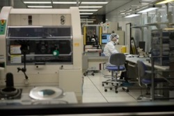
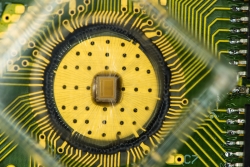
Celestica Inc., Toronto, announces the opening of its new microelectronics laboratory, an 1100-ft2, ISO Class-6 clean room with a controlled environment for temperature, humidity, and airborne particles. The laboratory provides new miniaturization solutions using bare die packaging technologies. The goal is to reduce production costs, enhance signal integrity, and improve thermal performance for high-reliability applications.
The new facility will enable start-ups, small and medium enterprises (SMEs), and large original equipment manufacturers to quickly commercialize their latest ideas for miniaturizing products through prototyping to volume production.
The location of the laboratory is a strategic choice, with Toronto being the largest ICT (Information, Communication and Technology) hub in Canada. The laboratory will significantly bolster the infrastructure for product enablement in Canada, and may also be leveraged by global customers looking to commercialize a product. Start-ups, SMEs, and OEMs can now have quick access to talent and the technologies in this facility.
“The new microelectronics laboratory complements our existing capabilities in Toronto including our materials laboratory and surface mount technology manufacturing,” said Shawn Blakney, Senior Director, Technology and Innovation. “As we look to the future, microelectronics will play an increasing role in technology, and with this new capability, we can help our customers to keep up with the pace of change and stay competitive in their markets.”