Imec, Belgium, has announced a joint development project with Coventor, Cary, N.C., that will enable faster and more optimized development of advanced manufacturing technology in the 3D device architecture era, extending down to Imec’s 10- and 7-nm processes.
To adopt the 7-nm node, the industry needs to select the optimal layout, as well as optimize process step performance and control methodology. Using Coventor’s SEMulator3D platform, engineers from Imec and Coventor are working together to reduce silicon learning cycles and development costs by down-selecting the options for development of next-generation manufacturing technologies.
The SEMulator3D platform is an integrated set of modeling tools with enhanced visibility, accuracy, and performance that enables engineers to interactively model and simulate a wide range of manufacturing effects in software before committing to expensive test chips.
At Imec, process and integration experts have connected optical lithography simulations with Coventor’s SEMulator3D virtual fabrication platform to explore FinFET scaling to the 7nm node and to compare the process window marginalities in several dense SRAM designs using Spacer Assisted Quadruple Patterning and either multiple immersion or EUV patterning cut/keep solutions.
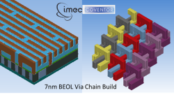
Moreover, a Spacer-Assisted Quad Patterning scheme for 7nm dense interconnect was devised using SEMulator3D, and process window marginalities for an immersion based multiple block patterning solution were analyzed. Additional collaboration will focus on the predictive modeling of Directed Self-Assembly for advanced patterning.