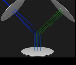
Engineers from Carl Zeiss Microscopy, Germany, presented a discussion of multi-beam scanning electron microscopes as tools for imaging semiconductor layers in less time at the ASM International ISTFA 2019 conference in Portland, Oregon. Commercial multi-beam SEMs are currently being evaluated for metrology and inspection workflows in the semiconductor industry. The technical setup of the multi-beam SEM is depicted in the diagram.
The multi-beam SEM circumvents the throughput limitations of standard single-beam SEMs by using multiple electron beams in parallel. Increasing the speed of a single-beam SEM could be achieved by faster scanning, which in turn would require higher beam current to still generate enough signal from the sample. Due to electron-electron interactions, this will impair the spot size of the electron beam and therefore the achievable resolution.
However, by spreading the current over multiple beams, these limitations can be avoided. Today, two different systems with 61 and 91 beams and equipped with a standard 100 mm SEM sample stage are commercially available. Given the increasing need for imaging larger areas in even shorter time frames, further throughput enhancements of the mSEM technology towards 331 beams are already on the way.
Title: Speeding up Chip Layer Imaging with a Multi-Beam SEM
A. L. Eberle, T. Garbowski, S. Nickell, D. Zeidler, Carl Zeiss Microscopy GmbH, Oberkochen, Germany