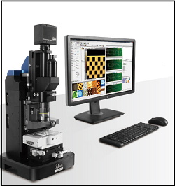
Park Systems, Santa Clara, Calif., and Imec, Belgium, have signed the second Joint Development Project (JDP) within four years to increase the development efforts for future generation in-line AFM metrology solutions.
The new JDP extends the collaboration to explore new frontiers of AFM metrology solutions for the wafer semiconductor sector. Enhanced possibilities of inline automated AFM in semiconductor research, such as surface roughness, critical dimension, and sidewall roughness, have been successfully explored in the first JDP. The second JDP targets multiple strategic developments to address the current metrological challenges of continuously downscaling the geometrical dimensions of devices and 3D assembly stacking.
After signing the first JDP in 2015, Park Systems officially joined Imec’s Industrial Affiliation Program. Ever since then, the interdisciplinary team of Park’s and Imec’s researchers and engineers has followed the goal of developing new protocols designed to increase production yield and device performance for the semiconductor industry. With a strong focus on practical problem-solving applications of the new JDP, the partners aim to deliver innovative 3D-metrology features for market challenges of ever smaller semiconductor devices.