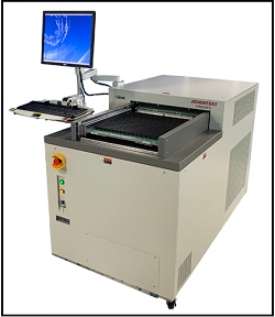
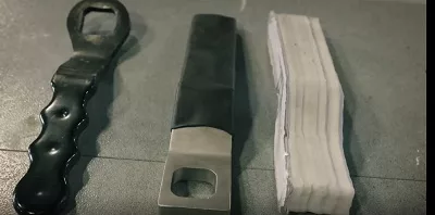
Engineers from Fischione Instruments, Export, Pa., described and compared different sample preparation techniques for solder joints in a presentation from the ASM International ISTFA 2019 conference in Portland, Oregon.
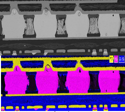
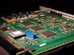
The packaging technologies of microelectronic flip chips involve solder joints that connect the chip and board. To guarantee reliability of microelectronic devices, the prediction of solder joint failures and their early state detection is critical. Both leaded and lead-free solder bumps are used as joints. An accurate, reliable, and easy-to-use investigation technique is critical for solder joint defect inspection in high-density microelectronic packaging.
The packaging technologies of microelectronic flip chips involve solder joints that connect the chip and board. To guarantee reliability of microelectronic devices, the prediction of solder joint failures and their early state detection is critical. Both leaded and lead-free solder bumps are used as joints. Because of constantly decreasing solder bump dimensions and pitch, defect detection and investigation is becoming more challenging.
An accurate, reliable, and easy-to-use investigation technique is critical for solder joint defect inspection in high density microelectronic packaging. One of the most critical failures of this joint is the loss of connectivity between copper pads and solder bumps, which appears in the form of cracks or delamination. These defects result from joint microstructural evolution induced by constant or cyclic loading conditions during device service.
The strain accumulated at the interface between solder bump and copper pad can lead to joint failure. Therefore, an understanding of the joint structure evolution and knowledge about the strain state at the joint interface can provide insight into the failure mechanism and prevent it in the future.
One of the most critical failures of this joint is the loss of connectivity between copper pads and solder bumps, which appears in the form of cracks or delamination. These defects result from joint microstructural evolution induced by constant or cyclic loading conditions during device service. The strain accumulated at the interface between solder bump and copper pad can lead to joint failure. Therefore, an understanding of the joint structure evolution and knowledge about the strain state at the joint interface can provide insight into the failure mechanism and prevent it in the future.
Solder bump joint failure investigation: From sample preparation to advanced structural characterizations and strain measurements
Pawel Nowakowski, Mary Ray, and Paul Fischione
E.A. Fischione Instruments, Inc., Export, Pennsylvania