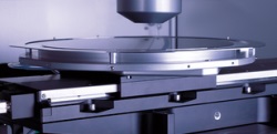
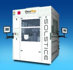
SÜSS MicroTec, Germany, has launched an excimer laser debonder, the ELD300, for the stress-free debonding of 200 and 300-mm 3D-IC wafers. The laser debonder can be used as a stand-alone, semi-automated system, or as an integrated process module in SUSS MicroTec’s XBC300 Gen2 platform. The debonding method relies on a 308-nm excimer laser to separate the glass carrier from a tape-mounted thin wafer. The ultraviolet light of the pulsed laser beam is absorbed in the adhesive or in an optional UV absorption layer within a few hundred nanometers.
The absorbed energy breaks the chemical bonds in the adhesive or absorption layer without generating thermal stress on the thin device wafer, so that the glass carrier can easily be lifted off after the debonding process. With the alternative module for mechanical peel-off debonding and the modules for post-debond cleaning of tape mounted thin wafers or carrier wafers, SUSS MicroTec’s XBC300 Gen2 platform offers a full solution package for debonding and cleaning applications.
The ELD300 mainly focuses on 2.5D and 3D-IC applications, but also addresses the requirements in the areas of 3D MEMS, CIS and power devices. The main competitive advantages of excimer laser-assisted debonding with the ELD300 are the short process times, which result in high throughput; the debonding selectivity of the process; the absence of mechanical or thermal stress on the thin device wafer; and eventually the high degree of automation that is essential for high-volume manufacturing.
“With the launch of the ELD300, we now offer two dedicated solutions for room-temperature debonding: mechanical peel-off and Excimer laser assisted processes,” says Frank P. Averdung, President and CEO of SUSS MicroTec AG.