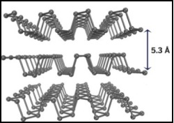
Researchers at the University of Southern California, Los Angeles, have shown that films of black phosphorus can be used to make radio-frequency transistors, components found in many telecommunication devices. Black phosphorus, the most stable form of the element at room temperature, has a structure that looks like a wrinkled version of graphite. Although black phosphorus has been known for a long time, it was not until this past year that researchers started exploring the use of the material for electronics.
Han Wang, an electrical engineer at the University of Southern California, says researchers are excited about black phosphorus because, unlike other two-dimensional materials, it both has a band gap and conducts charge fairly well. A material with a band gap can be switched between conducting and insulating states, lending devices such as transistors well-defined on and off states. This produces high-quality signals and saves power when the transistor is off. Materials with high charge mobility conduct charges well, and transistors made with them can switch on and off rapidly. Graphene has no band gap, but it does have superlative charge mobility. Meanwhile, other 2-D materials, such as molybdenum disulfide, have a band gap but have low charge mobility.
On the basis of what they and other researchers recently have learned about the material, Wang, Fengnian Xia of Yale University, and their colleagues built transistors made from a few layers of black phosphorus. These transistors can operate in the gigahertz range, switching on and off 20 billion times per second. Their performance is similar to that of transistors used in radio-frequency telecommunications circuits, such as those found in cell phones. Those transistors are made from silicon and other rigid semiconductors.
To make the devices, the researchers mechanically cleaved bulk black phosphorus into flakes. They selected flakes 6 to 10 nm thick and placed them on silicon wafers topped with a layer of silicon dioxide. To complete the transistors, they then used conventional methods to grow metal electrodes and a gate. The new transistors were quite large, about 300 nm wide. Simulations run by the team predict that if they can shrink the devices to 50 nm or smaller, the transistors should operate above 100 GHz.