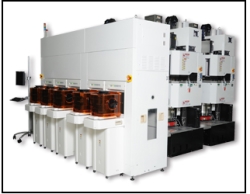
Hitachi High-Tech, Schaumburg, Ill., has developed the 9000 Conductor Etch Series to support next-generation devices at 20 nm and below that require double-patterning, 3D structures, and complex, high-precision processes. These processes include protective layer formation and finishing techniques for new materials. The new HHT 9000 platform utilizes Hitachi’s proprietary low-contaminant, high-speed transfer system for high productivity.
The linked common platform permits process flexibility and future expansion through its modular chamber design. Platform and user interface standardization will facilitate a smooth transition to 450-mm wafer sizes. The 9000 platform incorporates HHT’s new microwave ECR (Electron Cyclotron Resonance) plasma etching chamber that has been proven in high-volume manufacturing usage.