A new semiconductor manufacturing technology from Applied Materials, San Francisco, Calif., uses artificial intelligence, or AI, to spot mistakes in chips more effectively.
Ensuring that chips come off the factory line without mistakes in features that are only a few nanometers wide is critical to modern chip manufacturers. The new Applied tools are aimed at inspecting those chips at various times during the manufacturing process.
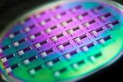
A new optical scanner called Enlight, essentially an advanced camera, scans a silicon wafer quickly for problem areas before an electron microscope zooms in for a closer look.
The problem Applied aimed to solve with AI is that electron microscopes are accurate but slow. An initial optical scan might find a million possible problem areas on a silicon wafer, and it would take an electron microscope days to examine each of those areas – and much of that time would go to waste, because only a fraction of the problem areas are what chip industry veterans call “killer” defects that would cause the chip to malfunction.
The new artificial intelligence technology, which Applied calls ExtractAI, only needs to check about 1,000 of those possible trouble spots with the electron microscope to predict where the biggest problems will be. Keith Wells, group vice president and general manager for imaging and process control at Applied, said the AI-powered check only takes about an hour.
“It’s economical for the customer to do that on every wafer,” Wells said. “We’re telling you with high confidence that these are the really killer defects.”
Applied has been testing the system with customers since last year and said it has generated more than $400 million in revenue so far.
For more information:
Applied Materials
https://www.appliedmaterials.com/