
Oxford Instruments Asylum Research released its new atomic force microscope package developed for battery research, the Cypher ES Battery Edition.
Continue reading

Oxford Instruments Asylum Research released its new atomic force microscope package developed for battery research, the Cypher ES Battery Edition.
Continue reading
According to researchers at Massachusetts Institute of Technology (MIT), Cambridge, Mass., engineers may now be able to figure out what’s going on inside a part—from an airplane wing to a medical implant—simply by observing properties of the material’s surface.
Continue reading
Evident Corp., Tokyo, announces the appointment of Eric Anderson as Interim CEO. Anderson, a member of the Office of the CEO at the time of his new appointment, takes on the responsibilities of Yoshitake Saito, who assumes the role of chairman.
Continue reading
Spirit Electronics, Phoenix, AZ, acquired Insight Analytical Labs, Colorado Springs, CO, to add device analysis services including destructive physical analysis, to its existing full-turnkey semiconductor supply chain services.
Continue reading
Testing the longevity of new electric vehicle battery designs could be four times faster with a streamlined approach, researchers at the University of Michigan have shown.
Continue reading
Scientists have searched, for decades, for a way to apply the exceptional analytical capabilities of neutrons to materials under pressures approaching those surrounding the Earth’s core. These extreme pressures can rearrange a material’s atoms, potentially resulting in interesting new properties.
Continue readingWith more than 50 years of innovation in mass spectrometry, JEOL, Japan, is pushing science a step further with their introduction of msFineAnalysis AI, an artificial intelligence-powered software designed to automatically perform qualitative GC-MS analysis.
Continue readingRigaku, Japan, leading provider of X-ray metrology solutions for semiconductor in-line processes, research and development, and high-volume manufacturing, has opened its first Semiconductor Metrology Technology Center in Sunnyvale, CA.
Continue readingPhysicists at the Australian National University are using nanoparticles to develop new sources of light that increase the frequency of light that cameras and other technologies see by up to seven times.
Continue reading
North Star Imaging, Rogers, MN, recently opened an x-ray inspection services laboratory in Orlando, Florida. The facility houses a vault with a 9 Million Electron Volt high energy CT X-ray system capable of scanning very large dense parts used in aerospace and aviation.
Continue reading
In experiments conducted at TU Wien, Vienna, extremely small pieces of gold, consisting of a few thousand atoms and with a diameter in the order of ten nanometers, are bombarded with highly charged ions. This makes it possible to change the shape and size of these gold pieces in a targeted manner. The effects of the ion bombardment were then studied in an atomic force microscope with surprising results.
Continue readingGraphene is extremely strong and good at conducting heat and electrical currents, making it an exceptionally versatile material. Yet, many properties of the material are still poorly understood – for the simple reason that the atoms they are made up of are very difficult to observe. A team of researchers from the University of Amsterdam (UvA) and New York University have now found a surprising way to solve this issue.
Continue readingMica, a common mineral found in granite, and has been extensively studied from geological, chemical, and technical perspectives. But recently a team from the Vienna University of Technology presented a study that explains the distribution of potassium ions on the mica surface. The researchers used a new type of atomic force microscope to conduct their investigation. Prior to this, the physical surface details of mica have never been studied on an atomic scale.
Continue readingOak Ridge National Laboratory (ORNL) researchers used neutron diffraction to identify a mechanism in a 3D-printed alloy—coined “load shuffling”—that could enable the design of better-performing lightweight materials for vehicles.
Continue reading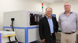 ACE Solution, Taiwan, the leader and the provider in customized test solutions to meet customer needs in electrical components, devices and system manufactures, launched the TZ6000 – a nondestructive wafer quality measurement tool for the compound semiconductor industry. Incorporated with TeraPulse Lx technologies from TeraView, United Kingdom, the TZ6000 achieves nondestructive wafer quality measurements of thickness, refractive index, resistivity, dielectric constant, surface/subsurface defects at selected positions and whole wafer scanning map.
Dr. JC Chen, VP of R&D of ACE Solution, commented “The quality of the semiconductor wafer determines the maximum achievable conversion efficiency to the final device. Subsurface damages (SSD) of semiconductor wafers are easily induced during surface machining process includes rough grinding, fine grinding, and chemical mechanical polishing. Current wafer inspection systems which rely on VIS/IR/UV optical inspection can analysis the surface properties of the wafer but not the SSD, due to their low penetration depth. Terahertz (THz) wave has higher penetration depth in semiconductor wafers as silicon, silicon carbide and gallium nitride. We developed the THz-based TZ6000 to meet the market need of nondestructive inspection of the compound semiconductor wafer.”
Dr. Philip F. Taday, head of applications and principal scientist of TeraView, commented “The TeraPulse Lx system is TeraView’s world-leading product family for terahertz analysis. It has been designed to meet the needs of the material inspection in imaging or spectroscopy applications, and is ideal for compound semiconductors. The system’s modular architecture and TeraView patented laser-gated photoconductive emitters and detectors gives the user both flexibility and expandability. The system also boasts an industry-leading 3,200 ps time-delay line, as standard.”
Steve Hsu, CEO of ACE Solution, commented “ACE Solution is the leading company in providing electrical precision test, integrating service and solution. It is great opportunity to collaborate with TeraView and incorporate the TeraPulse Lx module into TZ6000 system for nondestructive wafer quality inspection. TZ6000 has high flexibilities for various sizes and forms of wafers. It is provided with TeraView’s unique THz-TDS probe for simultaneous measurement of multiple parameters of wafer characterization. TZ 6000 has a user-friendly and graphic illustrate software for quality inspection in wafer manufacturing process and R&D.”
Dr. Don Arnone, CEO of TeraView, commented “This is another first from TeraView to have a close collaboration with ACE Solution to develop this product, and we are quite confident that this product will set a new standard in compound semiconductor wafer quality analysis and defect inspection. The TeraPulse Lx system is designed with a lightweight compact core unit which allows for easy transport between locations. Incorporated with TeraView’s TeraPulse Lx modules, we can address the growing needs of the compound semiconductor wafer industry with this product.”
Image – Left: TZ6000 System incorporated with TeraPulse Lx; Middle: Steve Hsu, CEO of ACE Solution. Right: Dr. Philip Taday, Head of Application of TeraView.
For more information:
ACE Solution, Co., Ltd.
https://www.acesolution.com.tw/en/index/
TeraView
 FormFactor, Inc., Livermore, Calif., a leading semiconductor test and measurement supplier, opened a new product demonstration and training center in San Jose, California. The facility is staffed with applications engineers and training professionals, and features
FormFactor engineering wafer probers, metrology systems and advanced probe cards outfitted to meet semiconductor test and measurement requirements from lab to fab, including solutions for advanced packaging, automotive high-power devices, high-speed digital, silicon photonics, and 5G/6G/millimeter-wave mobile devices.
“The opening of our new demonstration center provides easy access for our customers to see first-hand the benefits of our sophisticated wafer probe and metrology solutions,” said Amy Leong, senior vice president and chief commercial officer. “We are deeply committed to enabling industry innovation, and proud to offer this center to accelerate our customers’ success with personalized, hands-on training, product demonstration, and support.”
FormFactor’s new demonstration center is located in the heart of Silicon Valley and offers a product demonstration lab and clean room, presentation and training areas, service warehouse, office space and conference rooms. The new location complements the capabilities of FormFactor’s existing global demonstration centers in Europe and Asia, and recently opened Advanced Quantum Cryogenic Lab in Boulder, Colorado.
For more information:
FormFactor, Inc.
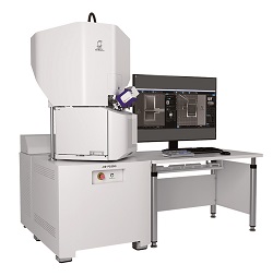 JEOL, Peabody, Mass., developed a new Focused Ion Beam (FIB) solution for preparing specimens prior to observing them in the Transmission Electron Microscope (TEM). The new JIB-PS500i is a multipurpose FIB-SEM that delivers the synergy of fast sample preparation, SEM imaging and EDS analysis in a single instrument.
The new FIB sample stage offers fast transitioning between processing and imaging, allowing for real-time feedback of specimen quality. With the ability to prepare samples thinner than 30nm, the FIB-SEM produces a sample suitable for superior atomic resolution imaging and analysis with STEM (Scanning Transmission Electron Microscope). A retractable STEM detector enables easy acquisition of bright field and dark field images during processing to precisely evaluate preparation of the TEM sample. The operator can easily prepare TEM specimens using the STEMPLING2 automatic TEM specimen preparation system, which allows unattended preparation of multiple samples.
A specially designed double-tilt sample holder, TEM-Linkage, enables seamless transfer from the FIB-SEM directly to the TEM.
A key advantage of the JIB-PS500i FIB is the large specimen chamber with an easy-access door. This design supports an efficient workflow and flexibility for a variety of samples and processes. The 5-axis full-eucentric large motor stage is designed to transport both large and multiple samples in the XY direction, and at a wide stage tilt and rotation range.
A new high current (up to 100 nA) FIB column is especially effective for large-area processing and analysis, which is ideal for semiconductor samples. The new FIB has high performance fine milling capabilities essential for quality lamella preparation imaging, EDS analysis, and 3D microscopy. The new JIB-PS500i has superior performance in the low kV range, as low as 0.5kV, essential for beam sensitive materials.
For more information:
JEOL USA, Inc.
 Scientists at the Argonne National Laboratory Advanced Photon Source (APS), Lemont, Ill., are exploring ways to analyze X-ray data faster and with more precision; its new TomocuPy software package has shown to be up to 30 times faster than the current practice.
Collecting and processing X-ray data faster is especially important for scientists working at the APS, which is about to undergo an extensive upgrade increasing the brightness of its X-ray beams by up to 500 times. Scientists use those beams to see ions moving inside batteries, for instance, or to determine the exact protein structure of infectious diseases. When the upgraded APS emerges in 2024, they will be able to collect that data at an exponentially faster rate.
To keep pace with the science, the analysis and reconstruction of that data — which shapes it into a useful form — will also have to get much faster before the APS Upgrade is complete. Argonne scientists have been working on multiple new methods using artificial intelligence to help speed up the timeline. Faster processes have been created for X-ray imaging and for determining important data peaks in X-ray diffraction data, to name a couple.
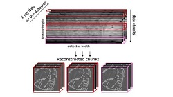
Argonne’s Viktor Nikitin, an assistant physicist working at the APS, has now unveiled a new way of reconstructing data taken through a process called tomography. Nikitin’s software package, called TomocuPy, builds on the current tools scientists use for tomography data. It improves the speed of the process by 20 to 30 times by leveraging computers equipped with graphics processing units (GPUs) and by reconstructing several chunks of data at once.
Nikitin’s innovations are important, and they involve an understanding of how tomography works: slice by slice. Tomography involves using an X-ray beam to observe multiple parts of the sample, extracting cross sections (or slices) from them, and then using a computer to reconstruct those slices into a whole. Nikitin’s TomocuPy builds a pipeline for processing those slices where the sequence of operations, such as reading and writing from hard disks and computations, can happen concurrently. Current methods examine each slice one at a time and put them together on the back end.
TomocuPy also takes advantage of the multiple processors within each GPU being used, and runs them all simultaneously. Stack up enough of these, and thousands of slices can be viewed in the time it would previously have taken to analyze one. Nikitin’s method also saves computing time by lowering the analysis precision of each GPU to match the output from the detector — if the output is 16-bit, he says, you don’t need 32-bit calculations to analyze it.
“Tomography is a lot of small operations, processing small images,” Nikitin said. “GPUs can do it up to 30 times faster. The previous method uses CPUs and doesn’t use the information pipeline that TomocuPy does, and it’s far slower.”
The GPUs in use for TomocuPy are often used for artificial intelligence applications, and can be adapted to work with machine learning algorithms. This is important, Nikitin said, because the eventual goal is experiments that can adjust to reconstructed data in real time.
Eventually, Nikitin said, the plan is to use artificial intelligence to help direct experiments, either by automatically zooming in on the interesting parts of a sample, or changing the environmental conditions like temperature and pressure in response to quickly reconstructed huge amount of APS Upgrade data. This will be possible, he said, with help from the massive supercomputers at the Argonne Leadership Computing Facility.
“We are building a fast connection between APS and ALCF,” he said. “By running TomocuPy on a supercomputer, we can do in a day what now can take up to a month.”
Image – TomocuPy allows for processing chunks of data concurrently in real time, making the entire reconstruction process faster. It moves chunks of data between processing units and returns the analyzed data to the storage drive much more quickly than current methods. Courtesy of: Viktor Nikitin/Argonne National Laboratory.
For more information:
Argonne National Laboratory
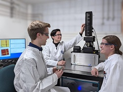 WITec GmbH, the originator of commercial Raman imaging systems, has delivered a new alpha300 R instrument to the Center for Solar Energy and Hydrogen Research (ZSW) Baden-Württemberg in Ulm, Germany. The Raman microscope will be used in the “Powder-Up!” pilot plant in Ulm, where cathode materials for lithium-ion batteries will be produced and the scalability of fabrication methods will be investigated.
Lithium-ion batteries are the primary enabling technology in the current shift toward electric mobility and their performance is almost exclusively determined by the materials used. ZSW is at the forefront of innovative energy storage development and is constructing a new building for the “Powder-Up!” pilot plant over the next twelve months. The new facility will focus on making improvements in the next generation of battery electrode materials, and on scaling up their manufacturing processes. This work is set to have far-reaching effects in terms of battery performance, resource use, and unit costs.
According to Dr. Margret Wohlfahrt-Mehrens, head of the Accumulators Materials Research department, “Raman microscopy is becoming a standard method in applied battery research. It quickly provides detailed information about how different electrode formulations function and degrade over charge cycles.”
WITec GmbH won the Europe-wide public tender due to the high chemical sensitivity, spatial resolution and acquisition speed of its Raman imaging systems. The alpha300 R microscope offers the added benefits of modularity for integrating hardware such as electro-chemical cells, and high sample throughput for compiling industrially relevant volumes of data.
The “Powder-Up!” facility, funded by the Baden-Württemberg Ministry of Economic Affairs, Labor and Tourism and the German Federal Ministry of Education and Research (BMBF), is the first of its kind in Europe. Material batches of up to 100 kilograms can be produced in the new plant. Such quantities are required to produce large battery cells for electric cars or stationary energy storage units.
Image – Florian Klein (left) and Leon Gläser (right) from the ZSW in Ulm together with WITec Application Scientist Dr. Ievgeniia Iermak (middle) during training on the new Raman microscope.
For more information:
Oxford Instruments Group
The Center for Solar Energy and Hydrogen Research Baden-Württemberg
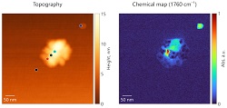 EAG Laboratories, San Diego, Calif., announced a new addition to its wide range of analytical techniques, NanoIR capabilities. NanoIR combines the nanometer scale spatial resolving capabilities of atomic force microscopy (AFM) with the chemical characterizing capabilities of infrared spectroscopy.
With this new capability, EAG scientists can provide clients with:
NanoIR spectra collected from the corresponding-colored locations indicated in the AFM image. Heterogeneities shown in the spectra are consistent with the chemical map, where the intensity of the PLGA ester peak (~1760 cm-1) varies across the particle and an additional ester species is detected (1730 cm-1).
Image – Data examples of PLGA nanoparticles deposited on mica. AFM height image (left) with colored markers indicating the corresponding analytical locations where spectra were obtained. A single wavenumber chemical map (right) taken at 1760 cm-1 reveals the ester-rich regions are detected only from the particles and are absent from the mica substrate. The chemical map highlights additional nanoscale heterogeneities that exist within the particles.
For more information:
EAG Laboratories
 AMETEK Gatan, Inc., Berwyn, PA, a global leader focused on enhancing and extending the operation and productivity of electron microscopes, announced the launch of the Cipher system—the first and only system that reveals, quantitatively, the distribution of lithium in conventional scanning electron microscopes (SEM) and dual beam instruments.
To successfully reach the energy reduction pledges of governments worldwide, researchers are developing lithium compounds and alloys to improve the capacity and storage of renewable energy technologies. Quantifying and understanding the micro-scale distribution of lithium now becomes ever more pressing during the development of this integral technology. Still, the observation of lithium in bulk materials at these length scales has remained tantalizingly out of reach.
“For many years, a method to reliably detect lithium has been considered the ‘holy grail’ of microanalysis. However, due to fundamental limits of physics, reliable measurement of the lithium content in critical materials such as those used in lithium-ion batteries has proved unachievable,” says David Stowe, SEM Product Manager, Gatan/EDAX. “With the launch of Cipher, a ground-breaking method is now available to reveal the lithium content in metallic alloys, compounds, and complex metal oxides down to low single-digit weight percentages.”
Using an original concept, the Cipher system combines quantitative analysis of backscattered electrons and the x-ray fluorescence signal to reveal lithium using a composition-by-difference method. Building on AMETEK’s expertise in detector technologies, researchers can now utilize a turnkey solution in the DigitalMicrograph software to collect quantitative data, correlate, and analyze lithium at the micro-scale.
“With this release of the Cipher system, we see the accelerated innovation that was foreseen by bringing the EDAX and Gatan brands together,” commented Narayan Vishwanathan, vice president and business unit manager of AMETEK Electron Microscopy Technologies. “We now bring a reliable method to detect lithium that will fast-track the development of improved renewable energy materials.”
For more information:
AMETEK Gatan

Scientists at the University of Auckland, New Zealand, are working at the level of atoms to create something unexpected: tiny metallic snowflakes. During their research, they discovered that interactions between the atomistic structures of various metals and liquid gallium cause differently shaped crystals to emerge.
Continue reading
Researchers at the University of Chicago’s Pritzker School of Molecular Engineering (PME) have now used a combination of high-powered electron microscopy and computational modeling to understand exactly what occurs, on an atomic level, when lithium-ion batteries degrade. Their research points toward one approach to designing longer-lasting lithium-ion batteries—by focusing on the carbon binder domain (CBD).
Continue reading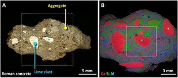 Researchers have spent decades trying to figure out the secret of Rome’s ultradurable ancient construction material, used in the famed Pantheon as well as aqueducts and seawalls that endured especially harsh environmental conditions. Now, a team of investigators from MIT, Harvard University, and laboratories in Italy and Switzerland, has made progress in this field, discovering ancient concrete-manufacturing strategies that incorporated several key self-healing functionalities.
For many years, researchers have assumed that the key to the ancient concrete’s durability was based on one ingredient: pozzolanic material such as volcanic ash from the area of Pozzuoli, on the Bay of Naples. This specific kind of ash was even shipped all across the vast Roman empire to be used in construction, and was described as a key ingredient for concrete in accounts by architects and historians at the time.
Under closer examination, these ancient samples also contain small, distinctive, millimeter-scale bright white mineral features, which have been long recognized as a ubiquitous component of Roman concretes. These white chunks, often referred to as “lime clasts,” originate from lime, another key component of the ancient concrete mix.
Upon further characterization of these lime clasts, using high-resolution multiscale imaging and chemical mapping techniques pioneered in Professor Admir Masic’s research lab at MIT, the researchers gained new insights into the potential functionality of these lime clasts.
Studying samples of this ancient concrete, he and his team determined that the white inclusions were made out of various forms of calcium carbonate. And spectroscopic examination provided clues that these had been formed at extreme temperatures, as would be expected from the exothermic reaction produced by using quicklime instead of, or in addition to, the slaked lime in the mixture. Hot mixing, the team has now concluded, was actually the key to the super-durable nature.
During the hot mixing process, the lime clasts develop a characteristically brittle nanoparticulate architecture, creating an easily fractured and reactive calcium source, which, as the team proposed, could provide a critical self-healing functionality. As soon as tiny cracks start to form within the concrete, they can preferentially travel through the high-surface-area lime clasts. This material can then react with water, creating a calcium-saturated solution, which can recrystallize as calcium carbonate and quickly fill the crack, or react with pozzolanic materials to further strengthen the composite material. These reactions take place spontaneously and therefore automatically heal the cracks before they spread. Previous support for this hypothesis was found through the examination of other Roman concrete samples that exhibited calcite-filled cracks.
To prove that this was indeed the mechanism responsible for the durability of the Roman concrete, the team produced samples of hot-mixed concrete that incorporated both ancient and modern formulations, deliberately cracked them, and then ran water through the cracks. Sure enough: Within two weeks the cracks had completely healed and the water could no longer flow. An identical chunk of concrete made without quicklime never healed, and the water just kept flowing through the sample. As a result of these successful tests, the team is working to commercialize this modified cement material.
Through the extended functional lifespan and the development of lighter-weight concrete forms, Masic hopes that these efforts could help reduce the environmental impact of cement production, which currently accounts for about 8% of global greenhouse gas emissions. Along with other new formulations, such as concrete that can actually absorb carbon dioxide from the air, another current research focus of the Masic lab, these improvements could help to reduce concrete’s global impact.
Image – Compositional and morphological characterization of ancient and modern lime clasts. (a) Optical micrographs showing the conspicuous bright white color of the lime clasts, which can easily be identified from large-area elemental mapping via SEM-EDS (b). Courtesy of Science Advances (2023). DOI: 10.1126/sciadv.add1602.
************
For more information:
 The speed at which an atomic force microscope moves across the surface of certain materials is influenced by the frictional properties of the substrate. One such example is graphene, which consists of a single layer of carbon atoms in a honeycomb arrangement. It is being examined with a view to potential use as a lubricating layer. Applications where a reduction of friction is desired include hard disks or moving components for satellites or space telescopes.
Previous studies have shown that a graphene ribbon can be moved across a gold surface with almost no friction. But if graphene is applied to a platinum surface, it has a significant impact on the measurable friction forces. Now, physicists from the University of Basel and Tel Aviv University have reported in the journal Nano Letters (“Velocity Dependence of Moiré Friction”) that, in this instance, the friction depends on the speed at which the tip of an atomic force microscope (AFM) is moved across the surface.
This finding is surprising because friction does not depend on speed according to Coulomb’s law, which applies in the macro world.
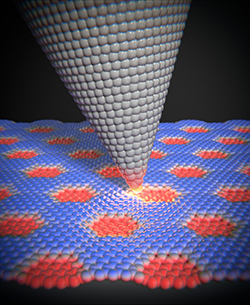
In conjunction with the platinum substrate, graphene no longer forms only the hexagonal honeycomb pattern of carbon atoms and instead forms superstructures known as Moiré superlattices. The surface is then no longer completely flat and exhibits a certain degree of roughness.
“If we move the AFM tip across this slightly corrugated surface at low speed, we measure a weak and almost constant frictional force,” explains Professor Ernst Meyer from the Swiss Nanoscience Institute and the Department of Physics at Basel University. “Above a certain threshold, however, the friction then increases with the speed of the AFM tip,” adds first author Dr. Yiming Song. “The larger the Moiré superstructure, the lower the threshold at which the friction becomes speed-dependent.”
The researchers found that there is greater resistance at the ridges of the Moiré superstructures during the movement of the tip. These ridges undergo elastic deformation due to the pushing tip before relaxing again when the pressure is sufficiently high. This effect results in greater frictional forces that increase with the speed of the tip. Simulations and an analytical model confirm the experimental findings obtained by this international team of researchers.
Image – The friction between the tip of an atomic force microscope and the Moiré superstructures depends on the speed at which the tip is moved across the surface. Courtesy of University of Basel.
************
For more information: