Skip to content

MIT researchers use AI to uncover atomic defects in materials

Researchers at the Massachusetts Institute of Technology built an AI model trained on 2,000 different semiconductor materials using data from a noninvasive neutron-scattering technique that can detect and classify up to six kinds of point defects in a material simultaneously, something that would be impossible using conventional techniques alone.

Continue reading

Constellium signs multi-year aluminum extrusions agreement with Airbus

Constellium, Issoire, France, announced a multi-year agreement with Airbus for the supply of aluminum alloy extrusions, reinforcing the company’s role as a long-term supplier of advanced aluminum solutions to the European airframer’s commercial and defense programs. Under the agreement, Constellium will provide Airbus with bars and a range of small and large extrusions manufactured in advanced aluminum alloys, including the company’s proprietary aluminum-lithium solution Airware®, all engineered to meet stringent quality requirements and optimized for the strength-to-weight performance demanded by aircraft structural applications. The extrusions will be produced at Constellium’s Issoire and Montreuil-Juigné facilities in France. “This agreement reflects Airbus’ trust in our advanced aluminum products and solutions, and in our quality performance, industrial reliability, and consistent supply continuity to support long-term aerospace programs,” said Philippe Hoffmann, president of Constellium’s Aerospace and Transportation business unit. “We are committed to continuing to grow our outstanding relationship with Airbus, leveraging our comprehensive product portfolio, proprietary solutions, unique manufacturing capabilities, and recycling expertise.” Constellium is a leading supplier of advanced aluminum products and solutions to the global aircraft, defense, and space markets, with proven industrial and recycling capabilities and an extensive portfolio of high-performance alloys, including the heat-treatable Airware® family used in next-generation airframe structures.

Read further here

Ferroelectric materials boost data storage potential

Researchers at Oak Ridge National Laboratory, Oak Ridge, Tenn., modified a commercial atomic force microscope with artificial intelligence to assemble and detect patterns in bismuth ferrite and analyze defects at the materials’ surface, advancing the understanding of these materials and enabling innovative data storage and computation methods.

Continue reading

Release of the Xtrology fully automated thin film inspection system

HORIBA STEC, Co., Ltd., Japan, released the fully automated thin film inspection system, Xtrology, that combines spectroscopic ellipsometry, Raman spectroscopy, and photoluminescence sensors making it possible to perform important inspections, such as film thickness measurement, defect analysis, and composition analysis of various wafers with a single instrument.

Continue reading

NSL Analytical Services relocates Metallurgical Testing Laboratory

NSL Analytical Services, Cleveland, Ohio, an independent analytical and metallurgical testing services company serving U.S. and global customers, announces a significant milestone in its growth trajectory with the relocation of one of its two Cleveland-area testing laboratories and the addition of high-temperature stress rupture testing to its offerings.

Continue reading

2D x-ray multilayer lens overcomes alignment challenge

A team of researchers have developed a new type of lens that focuses an x-ray beam to nanometer levels. The monolithic 2D multilayer Laue lenses (MLLs) can focus an x-ray beam to approximately 10 nanometers. The system overcomes the alignment challenges typically associated with these ultra-high resolution focusing optics. The 2D optics are based on advances in microfabrication. The optics provide a robust and compact approach for nanometer-scale resolution x-ray microscopy studies. This development was recognized with a Microscopy Today Innovation Award in 2022.

Continue reading

Probing subsurface materials via atomic force microscopy

A new nanoscience study, led by the Department of Energy’s Oak Ridge National Laboratory, takes a big-picture look at how scientists study materials at the smallest scales. Their research in subsurface nanometrology, the science of internal measurement at the nanoscale level, suggests quantum sensing could become the foundation for the field’s next era of discoveries.

Continue reading

Nanoindentation testing results found inconsistent

Nanoindentation testing is a high-precision indentation test technique that has advantages for nondestructive testing. However, researchers found that when testing the same sample with different Berkovich indenters, inconsistency still arises even if the indenters are regularly calibrated. This inconsistency poses challenges in accurately testing material hardness and comparing data from different laboratories.

Continue reading

TZ6000 – a nondestructive wafer quality measurement tool for the compound semiconductor industry

ACE Solution, Taiwan, the leader and the provider in customized test solutions to meet customer needs in electrical components, devices and system manufactures, launched the TZ6000 – a nondestructive wafer quality measurement tool for the compound semiconductor industry. Incorporated with TeraPulse Lx technologies from TeraView, United Kingdom, the TZ6000 achieves nondestructive wafer quality measurements of thickness, refractive index, resistivity, dielectric constant, surface/subsurface defects at selected positions and whole wafer scanning map.

Dr. JC Chen, VP of R&D of ACE Solution, commented “The quality of the semiconductor wafer determines the maximum achievable conversion efficiency to the final device. Subsurface damages (SSD) of semiconductor wafers are easily induced during surface machining process includes rough grinding, fine grinding, and chemical mechanical polishing. Current wafer inspection systems which rely on VIS/IR/UV optical inspection can analysis the surface properties of the wafer but not the SSD, due to their low penetration depth. Terahertz (THz) wave has higher penetration depth in semiconductor wafers as silicon, silicon carbide and gallium nitride. We developed the THz-based TZ6000 to meet the market need of nondestructive inspection of the compound semiconductor wafer.”

Dr. Philip F. Taday, head of applications and principal scientist of TeraView, commented “The TeraPulse Lx system is TeraView’s world-leading product family for terahertz analysis. It has been designed to meet the needs of the material inspection in imaging or spectroscopy applications, and is ideal for compound semiconductors. The system’s modular architecture and TeraView patented laser-gated photoconductive emitters and detectors gives the user both flexibility and expandability. The system also boasts an industry-leading 3,200 ps time-delay line, as standard.”

Steve Hsu, CEO of ACE Solution, commented “ACE Solution is the leading company in providing electrical precision test, integrating service and solution. It is great opportunity to collaborate with TeraView and incorporate the TeraPulse Lx module into TZ6000 system for nondestructive wafer quality inspection. TZ6000 has high flexibilities for various sizes and forms of wafers. It is provided with TeraView’s unique THz-TDS probe for simultaneous measurement of multiple parameters of wafer characterization. TZ 6000 has a user-friendly and graphic illustrate software for quality inspection in wafer manufacturing process and R&D.”

Dr. Don Arnone, CEO of TeraView, commented “This is another first from TeraView to have a close collaboration with ACE Solution to develop this product, and we are quite confident that this product will set a new standard in compound semiconductor wafer quality analysis and defect inspection. The TeraPulse Lx system is designed with a lightweight compact core unit which allows for easy transport between locations. Incorporated with TeraView’s TeraPulse Lx modules, we can address the growing needs of the compound semiconductor wafer industry with this product.”

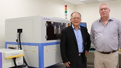
Image – Left: TZ6000 System incorporated with TeraPulse Lx; Middle: Steve Hsu, CEO of ACE Solution. Right: Dr. Philip Taday, Head of Application of TeraView.

For more information:

ACE Solution, Co., Ltd.

https://www.acesolution.com.tw/en/index/

TeraView

https://teraview.com/

Award winning adaptive measurement templates speed up identification of deformed components

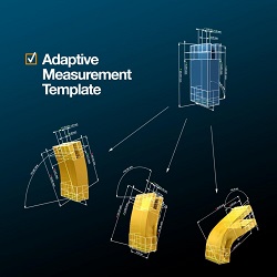
Leading software provider Volume Graphics, Germany, received a 2023 industry award for their Adaptive Measurement Template application that automatically compares original CAD intent against scan-based visualizations of parts, made with almost any material or manufacturing method, to assess quality and robustness. Volume Graphics’ Adaptive Measurement Templates has been named as one of the ten most innovative technologies for 2023 by a leading industry publication.

As CT scanning of parts becomes an increasingly routine quality-inspection step for manufacturers in automotive, aerospace, energy, medicine and other industries, the software that interprets that CT-scan data is becoming ever-more sophisticated, as well as more user-friendly.

An independent jury of machine-vision experts anonymously evaluated a shortlist of technology developments in image processing, metrology, embedded vision, and AI. The editorial team drew up the original list from around 30 products that stood out at trade fairs or in news articles over the past year. The jury then assigned points and selected the ten technologies with the highest total to be listed as Top Innovations. Products or solutions are selected because they enable more accurate, better, or simpler inspections for the industry.

Volume Graphics provides its Adaptive Measurement Templates in its latest versions of VGSTUDIO MAX, VGSTUDIO, VGMETROLOGY and VGinLINE software. These applications use data from CT-scanned objects to inspect and evaluate product quality. The shape-following templates speed up the identification of deformed components by allowing users to digitally apply metrics from their original CAD data or Product Manufacturing Information onto digital visualizations of the altered components, created from the CT scans.

The templates then highlight any differences between the original design and the as-manufactured-and-scanned part, and can be further applied to determine if such deviations are significant enough to affect performance or even cause rejection of the part.

This is highly valuable for the inspection of injection-molded parts and 3D-printed parts, which can often be out of tolerance and/or warped in such a way that a standard measurement plan, created on the nominal CAD object, cannot be applied easily or automatically to them. In such cases, correct analysis used to be possible only by applying time-consuming, local coordinate systems. The new Adaptive Measurement Templates apply dimensions and tolerances much more quickly, even to severely distorted parts, and can also inform design changes that improve final product quality.


For more information:

Volume Graphics

www.volumegraphics.com