Johnson Matthey and BP produces product for Fulcrum’s Sierra waste-to-fuels plant

Johnson Matthey, UK, has announced that their technology has enabled Fulcrum’s Sierra BioFuels Plant to successfully produce synthetic crude oil for clean transportation fuels.

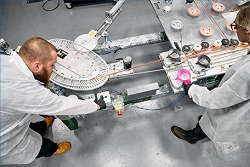
Using Johnson Matthey (JM) and BP’s FT CANS technology, the Sierra plant is the world’s first commercial-scale plant to use household rubbish as a feedstock that would otherwise be destined for landfill. The plant will produce synthetic crude oil, which is expected to ultimately be refined to approximately 11 million gallons of renewable, low-carbon transportation fuels each year from approximately 175,000 tons of landfill waste. JM and bp signed their first license with waste-to-fuels developer Fulcrum to use their award-winning FT CANS technology in 2018.

Read further here.


Tokamak Energy and Furukawa Electric Group strengthen relationship to progress commercial fusion energy

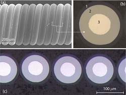
Furukawa Electric, Japan, has signed an agreement with Tokamak Energy to supply specialist high temperature superconducting (HTS) wire for its new advanced prototype fusion device, ST80-HTS.


Furukawa Electric Co., LtdTokyo, Japan and SuperPower Inc, New York, USA of Furukawa Electric Group, are expected to deliver more than several hundred kilometers of wire to the Oxford-based company for the next phase of construction. ST80-HTS will be the world’s first high field spherical tokamak using HTS magnets at scale and will utilize HTS wire developed and supplied by Furukawa Electric Group. This is a key stage in the path to Tokamak Energy’s fusion pilot plant which will demonstrate the capability to deliver clean electricity into the grid in the early 2030s, producing up to 200 MW of net electrical power.


HTS magnets are an essential enabler for the low cost, commercial operation and global deployment of spherical tokamak devices. They are essential for confining the fuel, which reaches temperatures above 100 million degrees Celsius. Tokamak Energy and Furukawa Electric Group are respectively leaders in the fields of HTS magnet design and superconducting wire development.


Read further here.

Superelastic conductor material with enhanced fatigue durability for implantable lead service

Fort Wayne Metals, Ind., has developed a new patent-pending technology to enhance the fatigue life of biostimulation leads.


These are used in devices like pacemakers, implantable cardioverter defibrillators, deep brain stimulators, and spinal cord and peripheral nerve stimulators under development in Fort Wayne Metals R&D. Conventional leads employ a composite DFT wire with a 35N LT alloy shell and a conductive silver core. By replacing the 35N LT alloy with superelastic or shape memory nitinol, dramatic improvements in strain-fatigue (and presumably service life) can be achieved. A polyimide coating is further applied to the wire, and with proper care can withstand the shape-setting head treatments needed to form nitinol into the desired lead components like cables and coil.


Read further here: https://www.fwmetals.com/services/r-d/rd-update/


Nupress and SPEE3D partnership brings patented cold spray technology to Australian manufacturers

SPEE3D, Australia, announced its WarpSPEE3D printer will be hosted at Nupress headquarters in Australia. Meaning local Australian manufacturers and businesses will be able to access the machine through a subscription without having to lease or purchase it.

This unique subscription model will provide Nupress’s existing clients in the mining, building, aerospace, defense, and medical industries, and other Australian manufacturers’ access to SPEE3D’s patented cold-spray technology. It will provide them the opportunity to source parts locally and quickly from a selection of 12 different metals.

Nupress is a leading manufacturer of precision machined components and assemblies with over 50 years of expertise. Together with SPEE3D, the game-changing subscription service will enable Nupress clients and other Australian manufactures to produce parts at the time of need, rather than waiting weeks or months via other supply chains. Because metal parts can now be sourced locally, this will help manufacturing companies improve their operations and reduce costs – many of which have been impacted negatively due to ongoing global supply chain issues. The subscription model offers one to six slots, each delivering 25 hours per month of printing for 12 months.

“Democratizing access to SPEE3D’s WarpSPEED printer will help solve real-world problems around broken supply chains, manufacturing challenges, and massive delays for some of the world’s most significant industries. Local Australian companies can now access our technology thanks to Nupress, enabling smaller production runs, prototyping needs, material developments, and other advanced manufacturing capabilities,” said Steven Camilleri, Co-Founder, and CTO of SPEE3D.


Image – WarpSPEE3D, the technology that will be available at Nupress on a subscription-based service for local Australian organizations.


For more information:

Nupress

https://www.nupress.com.au/


SPEE3D

https://www.spee3d.com/


Titomic successfully raises $5.1 million

Cold spray additive manufacturing company Titomic, Australia, announced it raised $5.1 million through a share placement, including $2.2 million from its existing strategic investor and joint venture partner Repkon.

Titomic Directors Herbert Koeck and Dag Stromme were also significant investors in the round, it said.

Managing Director Koeck told investors that the new funds would give Titomic “an ability to continue to execute on joint ventures, machine sales, workflow solutions, application development and reseller opportunities.”

He added that Repkon’s “additional strategic investment builds on our strong relationship, with JV and reseller agreements in place, as we move forward with the integration of Titomic’s TKF process and Repkon’s flowforming capabilities for the production and distribution of high-performance barrels in the defense sector.”


Image – Courtesy of Titomic.


For more information:

Repkon

https://www.repkon.com.tr/en


Titomic

https://titomic.com/


Oerlikon invests in its Surface Solutions business with a new state-of-the-art assembly and production site in Switzerland

Oerlikon, Switzerland, a global leader in surface technology, polymer processing, and additive manufacturing, is planning a new state-of-the-art assembly and production site for its surface solutions and equipment businesses. The Group’s current locations in Wohlen, Dottikon and Winterthur will be merged at the Reichhold Campus in the canton of Aargau. With this investment, Oerlikon is affirming its commitment to Switzerland as a business location.

Oerlikon is developing a new, attractive site on the Reichhold Campus in Hausen/Lupfig together with HIAG Immobilien Schweiz AG. This state-of-the-art site will provide customers with Oerlikon Metco thermal spray solutions, including equipment assembling and production services. The new location will enable further improvements in productivity and more optimized operational processes.

The Campus Reichhold site, spread across a total of around 14,500 m2 of production and office space, will also serve as a sales and distribution center for the materials product line, house an IT competence center, and offer around 230 employees an attractive workplace. A strong focus will be placed on sustainability and innovative approaches to future-oriented energy, mobility and utilization concepts.

The application for the building is planned to be submitted in the Summer of 2023. Construction is scheduled to start in the Spring of 2024, and the new location is expected to be ready for moving in from mid-2025 onward. At the current sites, all activities and work will continue as usual. According to the current plan, the move will begin in the summer of 2025 and will take place gradually to ensure the continued processing of all customer orders.


Image – Courtesy of Nau.ch / Wener Rolli and HAIG.


For more information:

HIAG Immobilien Schweiz AG

https://www.hiag.com/


Oerlikon

https://www.oerlikon.com


Augmented reality-enabled cold spray robot from AFRL wins defense tech award

The Air Force Research Laboratory and the Advanced Robotics for Manufacturing Institute won the Defense Manufacturing Technology Achievement Award for leading a development of a cold spray robot used in aerospace equipment refurbishment.

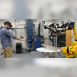
Dubbed ARRI, the augmented reality-enabled cold spray robot was created at AFRL’s Materials and Manufacturing Directorate. ARRI functions with the Microsoft Hololens virtual reality headset, which helps the human user control where a thermal coating should be applied on an aerospace workpiece undergoing rehabilitation.

In addition to funding from the laboratory, cost sharing agreements were signed with members of the ARM Institute as well as project integrators at the University of Connecticut and Titan Robotics to complete the project.

ARRI was installed in July at Warner Robins Air Logistics Complex, Robins Air Force Base in Georgia. WR-ALC invested $1.6 million to obtain two more ARRI-enabled controllers from Titan Robotics.

“The ARRI robot allows someone with no cold spray experience to be trained in about a day. The system also speeds up the time it takes to spray, reduces fixture costs, and improves capacity,” shared Shane Groves, robotics and automation expert at WR-ALC. He noted that the technology reduced training time by 90 percent and can save $600,000 in annual depot operating costs.


Image – Courtesy of: AFRL.


For more information:

Advanced Robotics for Manufacturing Institute

https://arminstitute.org/


AFRL

https://www.afrl.af.mil/


Titan Robotics

https://titan3drobotics.com/


University of Connecticut

https://uconn.edu/


Spray Tips: Mechanical methods for producing thermal spray powders

The purposes of milling are many: to reduce the size of particles or agglomerates, to eliminate particle segregation or preferred orientation in single-phase particles or in multicomponent powder systems, and to homogeneously disperse the many components.

Three basic stages are followed during the milling process: an initial rapid reduction in the size of aggregates, fracture of individual particles, and eventually, reagglomeration of fine particles after extended milling. The initial aggregates may be approximately 10 to 15 μm (0.4 to 0.6 mil), and these will be reduced to fines of the order of 0.1 μm (0.004 mil).

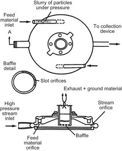
The problems of mill wear have been partially overcome with fluid energy and shear mills. The operating principle of these devices is similar. The material is incorporated into either a gas or a liquid stream, and two streams of the fluidized material are forced to be coincident. The individual particles collide and abrade each other. The grinding efficiency of these mills is high and there is minimum contamination, because there is little high-velocity contact with the walls of the mill. The major problem with this type of mill is the necessity to separate a fine particle from the fluidizing gas or liquid. The required filtering system adds to the complexity of the milling operation.


Image – Fluid energy mill.

This information is from ASM Handbooks Online, Vol. 5A: Thermal Spray Technology, Coating Structures, Properties, and Materials. To find this information (subscription required), click on the link below and scroll down to Figure 2.
https://dl.asminternational.org/handbooks/edited-volume/12/chapter/133823/Feedstock-Material-Considerations-for-Thermal


Milestone for light-driven electronics: excitons generated in a topological insulator for the first time

An international team of scientists collaborating within the Würzburg-Dresden Cluster of Excellence ct.qmat, Germany, has achieved a breakthrough in quantum research – the first detection of excitons (electrically neutral quasiparticles) in a topological insulator. This discovery paves the way for a new generation of light-driven computer chips and quantum technologies. It was enabled thanks to smart material design in Würzburg, the birthplace of topological insulators. The findings have been published in the journal Nature Communications.

In their search for novel materials for future quantum technologies, scientists from the Cluster of Excellence ct.qmat – Complexity and Topology in Quantum Matter – at the two universities in Würzburg and Dresden are concentrating on topological insulators, which enable the lossless conduction of electrical current and robust information storage. The first experimental realization of this materials class took place in Würzburg in 2007, prompting a worldwide research boom in solid-state physics that continues to this day.

Previous concepts for using topological insulators are based on the application of electrical voltages in order to control currents – an approach adopted from conventional computer chips. However, if the exotic material properties are based on electrically neutral particles (which are neither positively nor negatively charged), an electric voltage no longer works. Such quantum phenomena therefore require other tools if they are to be generated at all – for example, light.

An international research team headed by Professor Ralph Claessen, quantum physicist from Würzburg and co-spokesperson of ct.qmat, has now made a crucial discovery. “For the first time, we’ve been able to generate and experimentally detect quasiparticles known as excitons in a topological insulator. We’ve thus created a new toolkit for solid-state physics that can be used to control electrons optically.” As Claessen emphasizes, “This principle could become the basis for a new type of electronic components.”

Excitons are electronic quasiparticles. Although they seem to behave like independent particles, they actually represent an excited electronic state that can only be generated in certain types of quantum matter. “We created excitons by applying a short light pulse to a thin film consisting of just one single layer of atoms,” explains Claessen. What’s unusual about this, he says, is that the excitons were activated in a topological insulator – something that wasn’t possible before. “This has opened up a completely new line of research for topological insulators,” adds Claessen.

The right starting material is crucial – in this case bismuthene. “It’s the heavy sibling of the miracle material graphene,” says Claessen, who first tailored the topological insulator in the lab five years ago. “We’re the global leaders in this field,” he adds. “Due to our sophisticated materials design, the atoms of the single layer of bismuthene are arranged in a honeycomb pattern, just like graphene. The difference is that bismuthene’s heavy atoms make it a topological insulator, meaning it can conduct electricity along the edge without loss – even at room temperature. This can’t be done by graphene.”

For about ten years, excitons have been investigated in other two-dimensional semiconductors and regarded as information carriers for light-driven components. “For the first time, we’ve managed to optically excite excitons in a topological insulator. The interaction between light and excitons means we can expect new phenomena in such materials. This principle could be used, for example, to generate qubits,” says Claessen.

Qubits are computing units for quantum chips. They’re far superior to traditional bits and allow to solve tasks within minutes for which conventional supercomputers would literally take years.i Using light instead of electrical voltage enables quantum chips with much faster processing speeds. The latest findings therefore pave the way for future quantum technologies and a new generation of light-driven devices in microelectronics.

Image – Three excitons (pairs consisting of an electron and an electron hole) on the topological insulator bismuthene. Due to the honeycomb atomic structure, electrons can only flow along the edges. This topological effect allows current to flow without resistance. Researchers from ct.qmat have managed to generate excitons in a topological insulator for the very first time, paving the way for novel light-driven components – and possibly even the realization of qubits. Courtesy of Jörg Bandmann/ct.qmat.


For more information:

Würzburg-Dresden Cluster of Excellence ct.qmat

https://www.ctqmat.de/en


Imec enables tight standard cell boundary scaling using a two-level semi-damascene integration scheme

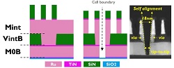
Imec, Belgium, a world-leading research and innovation hub in nanoelectronics and digital technologies, presents a semi-damascene integration approach for implementing the vertical-horizontal-vertical (VHV) scaling booster – intended to enable 4-track (4T) standard cells. The semi-damascene process enables cell boundary scaling down to 8nm tip-to-tip (T2T) in the middle-of-line (MOL) layers, providing self-aligned edges.

This provides a booster that designers can use for packing standard cells tighter, representing a 21 percent area gain over 5T designs. The novel routing scheme, along with the semi-damascene integration approach, will be critical to gradually push the logic scaling roadmap well into the Å era.

For a long time, the MOL, which provides the connection between the front-end-of-line (FEOL) and back-end-of-line (BEOL), has been organized as a single-layer contact. But currently, it is expanding into several layers, including, for example, the Mint and Vint layers. These MOL layers carry the electrical signals from the transistor’s source, drain, and gate to the local interconnects and vice versa.

Imec recently introduced a novel standard cell routing architecture called VHV, which involves the introduction of an extra MOL layer (M0B) as a scaling booster to enable 4T standard cell designs. With this booster, the first three routing layers in the standard cell follow a VHV routing style instead of the traditional HVH routing style in 5T standard cells. However, the novel two-level MOL VHV scaling booster is challenging from a process integration point of view, mainly arising from the tight boundary between neighboring 4T standard cells. The cell boundary requires a tight T2T between adjacent MOL M0B lines and two vias (VintB) facing each other with well-defined via edges – all at a minimum distance of one critical dimension (CD) of the top Mint layer. This means that the T2T and VintB via distance will need to be gradually reduced from ~24nm to ~8nm for upcoming technology nodes. This can no longer be achieved using a direct lithographic print but requires a self-aligned patterning strategy instead.

Researchers defined the tight boundary between adjacent standard cells using a two-level semi-damascene approach involving a direct metal etch. Zsolt Tőkei, program director of nano-interconnects and fellow at imec said, “Roughly speaking, we start from conventionally defined continuous lines and wider vias and, once two metal layers are finished, we split them into two, using the top 16-18nm pitch Mint layer as a hard mask for the final patterning step. This results in 3 edges (of Mint, VintB, and M0B) that are simultaneously self-aligned. With our Ru-based two-level test vehicle, we obtained an average via CD of 10.5nm and M0B T2T as tight as 8.9nm – a key achievement.” Imec researchers complemented structural validation with an initial electrical characterization of line resistance and isolation properties.

“The VHV routing scheme is a critical scaling booster to enable cell boundaries at the A10, A7, A5, A3 technology nodes,” adds Tőkei. “It also applies to future device architectures such as nanosheet, forksheet, and CFET. By extending semi-damascene from the BEOL towards the MOL, we have now also found a way to integrate this promising booster. More detailed investigations will, however, be needed, and for that purpose, imec is taping out a new dedicated mask.”


Image – (Left/middle) Schematic representation of the semi-damascene process flow used to test the key features of VHV. (Right) TEM image of the test vehicle after the final Ru etch: T2T M0B and VintB via are self-aligned to the 18mn pitch Mint layer.


For more information:

Imec

www.imec-int.com


Applied Materials launches ‘Singapore 2030’ plan to expand its operations and innovation capabilities

Applied Materials, Inc., Santa Clara, Calif., announced “Singapore 2030” – a multi-faceted plan to expand its operations in Singapore over the next eight years. The plan is targeted at strengthening the company’s global manufacturing and R&D capabilities, broadening technology ecosystem partnerships in Singapore and promoting local workforce development.

“For the past 30 years, Singapore has been a strategic hub for Applied Materials, and we are excited to build on our success with new investments that will strengthen our ability to support the semiconductor industry on its path to becoming a US$1 trillion market by the end of the decade,” said Gary Dickerson, president and CEO of Applied Materials. “We look forward to working with the Government of Singapore and the vibrant technology ecosystem to create opportunities for mutual growth that will benefit the global semiconductor industry.”

With the semiconductor industry entering a new wave of growth fueled by digital transformation of the economy, Applied has announced its intention to make multi-billion-dollar investments in its innovation infrastructure in the United States and to expand its global manufacturing capacity. As part of Singapore 2030, Applied Materials held a groundbreaking ceremony for an expansion of its regional hub in Singapore, which is home to Applied’s largest factory outside of the United States. This investment of hundreds of millions of U.S. dollars will strengthen the company’s ability to meet growing customer demand in the years ahead.

In addition, the company will invest to bolster its R&D capabilities in Singapore with a focus on accelerating commercialization of new technologies and services that improve chip power, performance, area, cost and time-to-market (PPACt). One example is the research collaboration between Applied and the Institute of Microelectronics (IME), a research institute of Singapore’s Agency for Science, Technology and Research (A*STAR), focused on hybrid bonding and other emerging, 3D chip integration technologies.

As a top employer, Applied will help enable a future-ready workforce for Singapore’s semiconductor equipment industry through enhanced training and advanced education programs. This includes an initiative with the Singapore Institute of Technology where Applied employees gain access to tailored learning modules in areas including AI and machine learning, smart manufacturing, robotics and automation, data science, and more.

Applied Materials established its presence in Singapore in 1991 with a small sales and service site that has grown to become a major manufacturing and regional operations hub with a workforce of more than 2,500. In 2019, Applied received the Distinguished Partner in Progress Award from the Government of Singapore in recognition of the company’s outstanding contributions and commitment to the country.


For more information:

Applied Materials, Inc.

www.appliedmaterials.com


Blocking radio waves and electromagnetic interference with the flip of a switch

Researchers in Drexel University’s College of Engineering have developed a thin film device fabricated by spray coating that can block electromagnetic radiation with the flip of a switch. The breakthrough, enabled by versatile two-dimensional materials called MXenes, could adjust the performance of electronic devices, strengthen wireless connections, and secure mobile communications against intrusion.

The team previously demonstrated that two-dimensional layered MXene materials – discovered just over a decade ago – when combined with an electrolyte solution, can be turned into a potent active shield against electromagnetic waves. This latest MXene discovery, reported in Nature Nanotechnology, shows how this shielding can be tuned when a small voltage – less than that produced by an alkaline battery – is applied.

MXene is a unique material in that it is highly conductive making it perfectly suited for reflecting microwave radiation that could cause static, feedback, or diminish the performance of communications devices. But its internal chemical structure can also be temporarily altered to allow these electromagnetic waves to pass through.

This means that a thin coating on a device or electrical components prevents them from both emitting electromagnetic waves, as well as being penetrated by those emitted by other electronics. Eliminating the possibility of interference from both internal and external sources can ensure the performance of the device, but some waves must be allowed to exit and enter when it is being used for communication.

The key to eliciting bidirectional tunability of MXene’s shielding property is using the flow and expulsion of ions to alternately expand and compress the space between material’s layers, like an accordion, as well as to change the surface chemistry of MXenes.

With a small voltage applied to the film, ions enter – or intercalate – between the MXene layers altering the charge of their surface and inducing electrostatic attraction, which serves to change the layer spacing, the conductivity and shielding efficiency of the material. When the ions are deintercalated as the current is switched off, the MXene layers return to their original state.

The team tested 10 different MXene-electrolyte combinations, applying each via paint sprayer in a layer about 30 to 100 times thinner than a human hair. The materials consistently demonstrated the dynamic tunability of shielding efficiency in blocking microwave radiation, which is impossible for traditional metals like copper and steel. And the device sustained the performance through more than 500 charge-discharge cycles.

These results indicate that the MXene films can convert from electromagnetic interference shielding to quasi-electromagnetic wave transmission by electrochemical oxidation of MXenes. The MXene film can potentially serve as a dynamic EMI shielding switch.
For security applications, the team suggests that the MXene shielding could hide devices from detection by radar or other tracing systems. The team also tested the potential of a one-way shielding switch. This would allow a device to remain undetectable and protected from unauthorized access until it is deployed for use.

The next step for the team is to explore additional MXene-electrolyte combinations and mechanisms to fine-tune the shielding to achieve a stronger modulation of electromagnetic wave transmission and dynamic adjustment to block radiation at a variety of bandwidths.


For more information:

Drexel University

https://drexel.edu


Chipletz selects Siemens’ EDA solutions for its smart substrate IC packaging technology

Siemens Digital Industries Software, Plano, Texas, announced that Chipletz, an innovative fabless substrate startup, has selected Siemens as its strategic electronic design automation (EDA) provider for the development of its groundbreaking Smart Substrate products.

After an extensive technical evaluation of available solutions, Chipletz selected a suite of Siemens’ industry-leading EDA tools for the design and verification of its Smart Substrate technology, which facilitates the heterogeneous integration of multiple ICs in a single package for critical artificial intelligence workloads, immersive consumer experiences, and high-performance computing.

“The Chipletz vision is to revolutionize semiconductor in-package functionality through the development of advanced packaging technology that bridges the gap between the slowing of Moore’s Law and the rising demand for compute performance,” said Bryan Black, chief executive officer of Chipletz. “Our Smart Substrate designs, now in development, are very demanding. Siemens has demonstrated that they have the ideal technology for our needs.”

To design and verify the heterogeneous integration of multiple ICs into a Smart Substrate based package, Chipletz selected Siemens’ Xpedition Substrate Integrator software, Xpedition Package Designer software, Hyperlynx software and Calibre 3DSTACK software solutions.

“Siemens is honored to be selected by Chipletz as a primary semiconductor packaging design and verification supplier,” said AJ Incorvaia, senior vice president of Electronic Board Systems at Siemens Digital Industries Software. “The Chipletz Smart Substrate technology offers Chipletz customers a robust path to bring multiple ICs, even from different vendors, into a wide range of system-in-package configurations using Siemens’ design tools to deliver a high-performing and cost-effective end-product.”


For more information:

Chipletz

https://chipletz.com/


Siemens Digital Industries Software

https://www.sw.siemens.com/en-US/


AI discovers new nanostructures

Scientists at the U.S. Department of Energy’s (DOE) Brookhaven National Laboratory, Upton, N.Y., have successfully demonstrated that autonomous methods can discover new materials. The artificial intelligence (AI)-driven technique led to the discovery of three new nanostructures, including a first-of-its-kind nanoscale “ladder.” The research was published in Science Advances.

The newly discovered structures were formed by a process called self-assembly, in which a material’s molecules organize themselves into unique patterns. Scientists at Brookhaven’s Center for Functional Nanomaterials (CFN) are experts at directing the self-assembly process, creating templates for materials to form desirable arrangements for applications in microelectronics, catalysis, and more. Their discovery of the nanoscale ladder and other new structures further widens the scope of self-assembly’s applications.

“Self-assembly can be used as a technique for nanopatterning, which is a driver for advances in microelectronics and computer hardware,” said CFN scientist and co-author Gregory Doerk. “These technologies are always pushing for higher resolution using smaller nanopatterns. You can get really small and tightly controlled features from self-assembling materials, but they do not necessarily obey the kind of rules that we lay out for circuits, for example. By directing self-assembly using a template, we can form patterns that are more useful.”

Staff scientists at CFN, which is a DOE Office of Science User Facility, aim to build a library of self-assembled nanopattern types to broaden their applications. In previous studies, they demonstrated that new types of patterns are made possible by blending two self-assembling materials together.

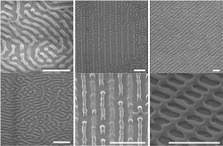
“The fact that we can now create a ladder structure, which no one has ever dreamed of before, is amazing,” said CFN group leader and co-author Kevin Yager. “Traditional self-assembly can only form relatively simple structures like cylinders, sheets, and spheres. But by blending two materials together and using just the right chemical grating, we’ve found that entirely new structures are possible.”

Blending self-assembling materials together has enabled CFN scientists to uncover unique structures, but it has also created new challenges. With many more parameters to control in the self-assembly process, finding the right combination of parameters to create new and useful structures is a battle against time. To accelerate their research, CFN scientists leveraged a new AI capability: autonomous experimentation.

In collaboration with the Center for Advanced Mathematics for Energy Research Applications (CAMERA) at DOE’s Lawrence Berkeley National Laboratory, Brookhaven scientists at CFN and the National Synchrotron Light Source II (NSLS-II), another DOE Office of Science User Facility at Brookhaven Lab, have been developing an AI framework that can autonomously define and perform all the steps of an experiment. CAMERA’s gpCAM algorithm drives the framework’s autonomous decision-making. The latest research is the team’s first successful demonstration of the algorithm’s ability to discover new materials.

“An old school way of doing material science is to synthesize a sample, measure it, learn from it, and then go back and make a different sample and keep iterating that process,” Yager said. “Instead, we made a sample that has a gradient of every parameter we’re interested in. That single sample is thus a vast collection of many distinct material structures.”

Then, the team brought the sample to NSLS-II, which generates ultrabright x-rays for studying the structure of materials and used the Soft Matter Interfaces (SMI) beamline in this study.

“One of the SMI beamline’s strengths is its ability to focus the x-ray beam on the sample down to microns,” said NSLS-II scientist and co-author Masa Fukuto. “By analyzing how these microbeam x-rays get scattered by the material, we learn about the material’s local structure at the illuminated spot. Measurements at many different spots can then reveal how the local structure varies across the gradient sample. In this work, we let the AI algorithm pick, on the fly, which spot to measure next to maximize the value of each measurement.”

As the sample was measured at the SMI beamline, the algorithm, without human intervention, created of model of the material’s numerous and diverse set of structures. The model updated itself with each subsequent x-ray measurement, making every measurement more insightful and accurate.

In a matter of hours, the algorithm had identified three key areas in the complex sample for the CFN researchers to study more closely. They used the CFN electron microscopy facility to image those key areas in exquisite detail, uncovering the rails and rungs of a nanoscale ladder, among other novel features.

From start to finish, the experiment ran about six hours. The researchers estimate they would have needed about a month to make this discovery using traditional methods.

“Autonomous methods can tremendously accelerate discovery,” Yager said. “It’s essentially ‘tightening’ the usual discovery loop of science, so that we cycle between hypotheses and measurements more quickly. Beyond just speed, however, autonomous methods increase the scope of what we can study, meaning we can tackle more challenging science problems.”

“Moving forward, we want to investigate the complex interplay among multiple parameters. We conducted simulations using the CFN computer cluster that verified our experimental results, but they also suggested how other parameters, such as film thickness, can also play an important role,” Doerk said.

The team is actively applying their autonomous research method to even more challenging material discovery problems in self-assembly, as well as other classes of materials. Autonomous discovery methods are adaptable and can be applied to nearly any research problem. “We are now deploying these methods to the broad community of users who come to CFN and NSLS-II to conduct experiments,” Yager said. “Anyone can work with us to accelerate the exploration of their materials research. We foresee this empowering a host of new discoveries in the coming years, including in national priority areas like clean energy and microelectronics.”

Image – Scanning-electron microscopy images depict novel nanostructures discovered by artificial intelligence. Researchers describe the patterns as skew (left), alternating lines (center), and ladder (right). Scale bars are 200 nanometers.


For more information:

Brookhaven National Laboratories

https://www.bnl.gov

Graphene nano-mechanical-switches could make our electronics even smaller and ultra-low-power

The quest for an ideal switching device for ultra-low power applications leads to an exploration of novel micro/nanoelectromechanical systems (M/NEMS) switches. This research has been driven by the superior performance of M/NEMS devices, such as ideally abrupt switching with zero off-state leakage, suitable for harsh and extreme environments, and very small footprints.

The suspended element of the NEMS switch is electro-mechanically moved by the applied electric field to establish physical contact with the counterpart of the switch, and thereby the conducting channel is established. However, an unacceptably high switching voltage of NEMS switches is the main obstacle to their practical use of it in low-power integrated circuits. In particular, sub-0.5 V switching voltage with a very small switch footprint, which is needed for ultra-low power circuits, has not yet been proven because of irreversible switching failure caused by surface adhesion. Moreover, once physical contact is created in NEMS switches, the switch contact area is increased, which leads to the domination of the surface attraction force over the mechanical restoring force; and as a result, permanent adhesion occurs.

To succeed in realizing NEMS switch for ultra-low power applications, the thickness of movable suspended material thickness has to be reduced as well as the switch contact adhesion in the ON state has to be overcome to reach the OFF state. The research team led by Dr. Manoharan Muruganathan (Former Senior Lecturer), and Professor Hiroshi Mizuta at the Japan Advanced Institute of Science and Technology (JAIST) proposed graphene-based NEMS switch research for this purpose.

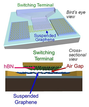
In the NEMS switch, the switching voltage is directly proportional to the suspended beam thickness, while the graphene monolayer is the thinnest material in the world today. Also, graphene shows cubic mechanical restoring force in the ON state, which is crucial to avoid stiction. Due to this unique characteristic, this research team pursued the graphene NEMS switch based on the doubly clamped suspended graphene beam with the hexagonal boron nitride (hBN) contact at the switching terminal.

Graphene-to-hBN binding strength is low due to its van der Waals (vdW) bonding nature, which will overcome the stiction issue of NEMS switches says the researcher Dr. Ngoc Huynh Van of Technical University of Denmark.  Based on the unique choice of materials and NEMS switch design, they have demonstrated sub-0.5 V switching characteristics with more than 50,000 hot-switching cycles of operation. Moreover, these NEMS switches show excellent switching characteristics, such as ~5 mV/dec switching slope, nearly-zero hysteresis, and >105 ON/OFF ratio, which meets the mainstream CMOS technology requirements.

These NEMS switches will play a vital role in various NEMS devices, sensors, NEM-CMOS hybrid integrated circuits, and ultralow-power applications.

For more information: Advanced Functional Materials

A new way to assess radiation damage in reactors

A new method could greatly reduce the time and expense needed for certain important safety checks in nuclear power reactors. The approach could save money and increase total power output in the short run, and it might increase plants’ safe operating lifetimes in the long run.
One of the most effective ways to control greenhouse gas emissions, many analysts argue, is to prolong the lifetimes of existing nuclear power plants. But extending these plants beyond their originally permitted operating lifetimes requires monitoring the condition of many of their critical components to ensure that damage from heat and radiation has not led, and will not lead, to unsafe cracking or embrittlement.

Today, testing of a reactor’s stainless-steel components — which make up much of the plumbing systems that prevent heat buildup, as well as many other parts — requires removing test pieces, known as coupons, of the same kind of steel that are left adjacent to the actual components, so they experience the same conditions. Or, it requires the removal of a tiny piece of the actual operating component. Both approaches are done during costly shutdowns of the reactor, prolonging these scheduled outages and costing millions of dollars per day.

Now, researchers at MIT and elsewhere have come up with a new, inexpensive, hands-off test that can produce similar information about the condition of these reactor components, with far less time required during a shutdown. The findings are reported today in the journal Acta Materiala in a paper by MIT professor of nuclear science and engineering Michael Short, Saleem Al Dajani a doctoral student at the King Abdullah University of Science and Technology (KAUST) in Saudi Arabia, and 13 others at MIT and other institutions.

The test involves aiming laser beams at the stainless-steel material, which generates surface acoustic waves (SAWs) on the surface. Another set of laser beams is then used to detect and measure the frequencies of these SAWs. Tests on material aged identically to nuclear power plants showed that the waves produced a distinctive double-peaked spectral signature when the material was degraded.

Short and Al Dajani embarked on the process in 2018, looking for a more rapid way to detect a specific kind of degradation, called spinodal decomposition, that can take place in austenitic stainless steel. This process can lead to embrittlement, cracking, and potential failure in the event of an emergency.

While spinodal decomposition is not the only type of degradation that can occur in reactor components, it is a primary concern for the lifetime and sustainability of nuclear reactors, Short says.

They decided to try a technique Short and his students and collaborators had expanded upon, called transient grating spectroscopy, or TGS, on samples of reactor materials known to have experienced spinodal decomposition as a result of their reactor-like thermal aging history. The method uses laser beams to stimulate, and then measure, SAWs on a material. The idea was that the decomposition should slow down the rate of heat flow through the material, that slowdown would be detectable by the TGS method.

However, it turns out there was no such slowdown. “We went in with a hypothesis about what we would see, and we were wrong,” Short says.

Instead, what showed up in the data was that, while a material would usually produce a single frequency peak for the material’s SAWs, in the degraded samples there was a splitting into two peaks.

Cast austenitic stainless steels like those used in reactor components are what’s known as duplex steels, actually a mixture of two different crystal structures in the same material by design. But while one of the two types is quite impervious to spinodal decomposition, the other is quite vulnerable to it. When the material starts to degrade, the difference shows up in the different frequency responses of the material, which is what the team found in their data.

The tests they did used large lab-based lasers and optical systems, so the next step, which the researchers are hard at work on, is miniaturizing the whole system into something that can be an easily portable test kit to use to check reactor components on-site, reducing the length of shutdowns.

Short hopes that this could help to enable the extension of power plant operating licenses for some additional decades without compromising safety, by enabling frequent, simple and inexpensive testing of the key components. Existing, large-scale plants “generate just shy of a billion dollars in carbon-free electricity per plant each year,” he says, whereas bringing a new plant online can take more than a decade. “To bridge that gap, keeping our current nukes online is the single biggest thing we can do to fight climate change.”

For more information: MIT

Researchers gain deeper understanding of mechanism behind superconductors

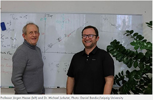
Physicists at Leipzig University have once again gained a deeper understanding of the mechanism behind superconductors. This brings the research group led by Professor Jürgen Haase one step closer to their goal of developing the foundations for a theory for superconductors that would allow current to flow without resistance and without energy loss. The researchers found that in superconducting copper-oxygen bonds, called cuprates, there must be a very specific charge distribution between the copper and the oxygen, even under pressure.
This confirmed their own findings from 2016, when Haase and his team developed an experimental method based on magnetic resonance that can measure changes that are relevant to superconductivity in the structure of materials. They were the first team in the world to identify a measurable material parameter that predicts the maximum possible transition temperature, a condition required to achieve superconductivity at room temperature. Now they have discovered that cuprates, which under pressure enhance superconductivity, follow the charge distribution predicted in 2016. The researchers have published their new findings in the journal PNAS.

“The fact that the transition temperature of cuprates can be enhanced under pressure has puzzled researchers for 30 years. But until now we didn’t know which mechanism was responsible for this,” Haase said.

He and his colleagues at the Felix Bloch Institute for Solid State Physics have now come a great deal closer to understanding the actual mechanism in these materials.

“At Leipzig University we have established the basic conditions needed to research cuprates using nuclear resonance, and Michael Jurkutat was the first doctoral researcher to join us. Together, we established the Leipzig Relation, which says that you have to take electrons away from the oxygen in these materials and give them to the copper in order to increase the transition temperature. You can do this with chemistry, but also with pressure. But hardly anyone would have thought that we could measure all of this with nuclear resonance,” Haase said.

Their current research findings could be exactly what is needed to produce a superconductor at room temperature, which has been the dream of many physicists for decades and is now expected to take only a few more years, according to Haase. To date, this has only been possible at very low temperatures around minus 150 degrees Celsius and below, which are not easy to find anywhere on Earth. About a year ago, a Canadian research group verified the findings of Professor Haase’s team from 2016 using newly developed, computer-aided calculations and thus substantiated the findings theoretically.

Superconductivity is already used today in a variety of ways, but it would be much easier and less expensive if superconductors operated at room temperature.

For more information: Leipzig University

Unlikely union of 3D-printed bronze and steel holds promise for jet engines

Skoltech researchers have used a 3D printer to fabricate samples of bronze-steel alloys previously unknown to materials science and investigated their mechanical characteristics. Blending the distinct properties of bronze and steel, the novel alloys could be used to manufacture combustion chambers for aircraft and rocket engines that would simultaneously benefit from steel’s ability to withstand extreme temperatures and bronze’s capacity to conduct heat away from the chamber and thus prevent the engine from overheating.

“3D printing is promising for manufacturing composite parts, endowed with the properties of the two distinct materials that make up the composite,” Associate Professor Igor Shishkovsky of Skoltech Materials explained. “Consider, for example, that steel is resistant to the high temperatures created by fuel combustion in an operating engine. This is great, but compared with bronze, steel is a modest thermal conductor, so the engine coolant cannot siphon heat away from it as effectively to prevent overheating and damage. Well, with 3D printing, you can actually get the best of both worlds by manufacturing a combustion chamber that seamlessly goes from being bronze on the inside for better temperature management to being steel on the outside for holding the structure together.”

Shishkovsky was the principal investigator on the study that reported the first-ever synthesis of a bronze-steel alloy using a 3D printing technique called direct laser deposition, which melts and fuses powdered ingredients by a laser beam at every successive point in the metal part just as it’s being created. In fact, the Skoltech team combined bronze and steel in two different ways, obtaining both so-called quasi-homogeneous alloys and sandwich structures. In the former, the two materials are more or less evenly intermixed throughout the sample, while the latter consists of a series of alternating 0.25-millimeter-thick layers of bronze and steel. The researchers used one type of steel but varied its content in the alloy from 25% to 50% and experimented with three different common varieties of bronze.

The study confirmed that the two materials fused well, without defects forming, and investigated the bronze-steel alloy’s structural and mechanical properties. To do this, the team grew vertical bars from the bottom up and examined their shape, chemical composition, and microstructure.

Finding no problems at this stage, the researchers proceeded to cut out tiny pieces from different parts of the samples and investigated their internal structure with optical and scanning electron microscopy. The main mechanical characteristics were then obtained in a wide range of mechanical tests of sandwich composites continued up to their destruction. These properties are reported for the first time.

The study’s first author Konstantin Makarenko, a fourth-year Ph.D. student at Skoltech Materials, said, “Now that we have confirmed that steel and bronze can be combined in an alloy and are compatible with 3D printing via direct laser deposition, and we know the mechanical characteristics of the new material, we can explore its possible applications.  Looking forward, I would like to manufacture and test a steel-bronze combustion chamber at Skoltech, but beyond that, other items are possible and other metal combinations could be used. The next step would be to create turbine blades made of a strengthened superalloy with cooling channels made of bronze. It’s all about combining the benefits of two distinct materials in one seamless product without any welding or other junctures.”

For more information: Materials & Design

Smallest earthquakes ever observed in micron-scale metals

On the micrometer scale, deformation properties of metals change profoundly due to the complex intermittent redistribution of lattice dislocations caused by external loading. This results in the formation of the uneven step-like surface upon deformation. To study this phenomenon, research groups of the Eötvös Loránd University of Budapest, Charles University of Prague and École des Mines de Saint-Étienne have developed a highly sensitive micromechanical platform, where weak elastic waves emitted by the specimen can be detected during the deformation of micron-scale pillars.

Compression experiments performed on such zinc single crystalline micropillars in a scanning electron microscope confirmed that these so-called acoustic signals indeed occur during strain bursts, so, this experiment allowed us, for the first time, to practically hear the “sound of dislocations.”

The acoustic signals are sampled with a rate of 2.5 MHz; therefore, they provide extremely detailed information on the dynamics of dislocations. The in-depth statistical analyses performed by the researchers revealed that strain bursts exhibit a two-level structure. What has so far been seen as a single plastic slip is, in fact, a result of several correlated events on a μs-ms timescale.

The most surprising outcome of the experiments is that this process, despite the fundamental differences between deformation mechanisms of metals and that of tectonic plates, was found to be completely analogous to earthquakes.

Acoustic signals emitted from the testpieces followed fundamental empirical laws established for main shocks and aftershocks in seismology, such as the Gutenberg-Richter and Omori laws.

“These results are expected to bear high technological impact since, for the first time, we were able to observe direct connection between acoustic signals and the plastic events that emitted them,” said Péter Dusán Ispánovity, assistant professor at Eövös Loránd University and head of the Micromechanics and Multiscale Modelling Research Group. “Since the measurement of acoustic emission is a frequent method for monitoring and locating material failure in technological applications, by providing fundamentally new information about the underlying physics our results are expected to contribute to the further development of this technique.”

The methodology can also be used to investigate other types of deformation mechanisms, such as twinning or fracture, so the results, which were published in Nature Communications, are expected to open up new vistas in the research of micromechanical properties of materials.

Image – On the micrometer scale deformation properties of metals change profoundly. The smooth and continuous behavior of bulk materials often becomes jerky due to random strain bursts of various sizes. Courtesy of Péter Dusán Ispánovity and Dávid Ugi.

************

For more information:

Eötvös Loránd University