Skip to content

Heralding the era of the cost-effective electric car

Currently, most cathode materials used in batteries for electric vehicles are layered oxides composed of nickel for over 60% of the transition metals. Using nickel-rich layered oxide is advantageous in securing the mileage of an electric vehicle due to its high energy density, but its usage is limited by instability in the supply and demand of nickel raw materials. As an alternative, researchers focused on spinel cathode materials that use manganese as the main element, considering manganese is traded at a price of about 1/17 of nickel in the international spot market; however, the rapid decline in lifespan was an obstacle to commercialization.

The Korea Institute of Science and Technology (KIST) announced that Dr. Jihyun Hong’s research team at the Energy Materials Research Center identified the cause of the rapid decline in life span-a chronic problem of high-capacity manganese-based spinel cathode materials. This team worked on significantly increasing the possibility of commercializing lithium batteries with manganese cathode materials as next-generation electric vehicle batteries.

Manganese-based spinel cathode materials can theoretically store energy with a high density comparable to nickel-based commercial cathode materials. Considering the price of metal raw materials, the energy density per price for manganese-based spinel cathode could reach 2.8 times that of nickel-based cathodes. However, when using the battery at full capacity, a rapid decrease in lifespan is observed; as a result, only approximately 75% of the theoretical value could be stored. It has been established that the trivalent manganese (Mn3+) formed during the charging and discharging process of manganese-based spinel cathode materials distorts the material’s crystal structure, leading to the elution of manganese into the electrolyte and eventually causing a reduction in the lifespan of the cathode material. As a result, most research has focused on suppressing the formation of trivalent manganese.

Contrary to mainstream academic theories, Dr. Hong’s team at KIST recently discovered that cathode materials exhibit excellent lifespan characteristics even when trivalent manganese is formed if the operating voltage range of the battery is adjusted. The research team utilized advanced material characterization techniques, including synchrotron radiation techniques, to interpret the phenomena that existing theories cannot explain. Through thorough analyses, for the first time, it was identified that the side reaction at the interface between the cathode material and electrolyte during the repeated charging and discharging process is the cause of lifespan reduction.

The research team further presented a key strategy to dramatically improve the lifespan of manganese-based materials by stabilizing the cathode-electrolyte interface. As an example of this strategy, introducing an EC-free electrolyte resulted in a 62% improvement in lifespan compared to commercial electrolytes. This improvement results in the highest capacity retention and rate capability among the performances of manganese-based spinel cathode materials simultaneously using nickel and manganese redox reactions reported so far.

For more information: Advanced Energy Materials
Investment in new plasma coating booths sees Sandon Global set the standard for anilox performance

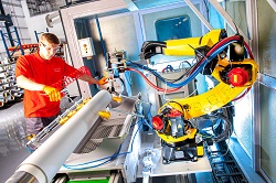
Leading anilox manufacturer Sandon Global (‘Sandon’) continues its program of investments with the installation of two new plasma coating booths at its UK headquarters.
The new booths will use proprietary thermal spray technology to produce anilox coatings that achieve increased hardness and lower porosity ratings than competing products, enabling printers to achieve premium quality print performance, reduce waste and minimize costs.

This new facility marks the latest in a range of investments by Sandon since the company moved to its new purpose-built premises. The site incorporates an in-house state-of-the-art metallurgical laboratory for research and development, enabling the company to further improve the quality of existing coatings and explore new developments.

Last year, the company invested in a powder manufacturing line to develop its own powder coating formulations that are tested using the latest generation equipment to maximize anilox performance. The new plasma coating investment now provides six meter capability to the business enabling it to tap into truly wide-web tissue, toilet roll, non-wovens, corrugated and textiles markets.

Richard Millington, Managing Director of Sandon Global, said: “At Sandon, we are investing in the future of anilox. We never stand still and have made significant progress since the move to our new headquarters with our unique R&D facilities. We’re focused on delivering next generation anilox solutions for a wide range of customers around the world and these latest capabilities change the game for us in terms of product performance and market access. We’re really excited about the progress we can now make in untapped markets.”


For more information:

Sandon Global

www.sandonglobal.com


Masan High-Tech Materials integrates global R&D activities under H.C. Starck Tungsten Powders‘ leadership

H.C. Starck Tungsten Powders, Germany, is bringing together the research and development activities within the Masan High-Tech Materials Group in an integrated structure. This will create an international innovation hub with a total of almost 40 highly specialized employees at the headquarters in Goslar and at Masan Tungsten LLC in Thai Nguyen, Vietnam.

The combined team focuses on application research in pyro- and hydrometallurgy, the optimization of existing processes and products, and the development of new, disruptive solutions and technologies.

The combined resources and capabilities are intended to make the company’s innovation processes even more powerful, flexible and effective. To achieve this, further investments in laboratory equipment and qualification measures are planned, especially at the Masan Tungsten LLC, APT Factory in Thai Nguyen.

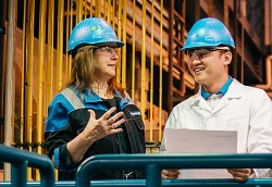
Image – Julia Meese-Marktscheffel, Director Technology and Innovation Global at H.C. Starck Tungsten Powders, with Dai Ngyuen Van, R&D Manager at Masan High-Tech Materials’ Thai Nguyen site.


For more information:

H.C. Starck Tungsten Powders

https://www.hcstarck.com

TC Energy: Keystone pipeline leak caused by welding flaw, bending stress

The Calgary-based TC Energy, formerly known as TransCanada, announced its initial findings into the December oil spill, stating the pipe failed due to a combination of factors, including bending and a weld flaw that was completed during its manufacturing.
“Although welding inspection and testing were conducted within applicable codes and standards, the weld flaw led to a crack that propagated over time as a result of bending stress fatigue, eventually leading to a instantaneous rupture,” it said in a statement, adding that the cause of the bending stress remains under investigation by a third party.

TC Energy added that metallurgical analysis found no issues with the strength or material properties of the pipe or manufactured fitting and that it was operating within its operation design and within its maximum operating pressure.

The leak was discovered on Dec. 7 about 20 miles south of Steel City, Neb., along the 2,687-mile pipeline that runs from the Canadian province of Alberta into the United States. The break was found near where it spilts into two arms with on running east into Illinois and the other south down to Houston, Texas.

The leak was found feeding oil into a Washington County, Kan., creek, with initial estimates putting the size of the leak at about 14,000 barrels. The company recently reduced that estimate to 12,937 barrels, for about 543,350 gallons of oil, making it the Keystone Pipeline’s largest spill.

The company also said that it estimates the clean-up costs to be about $420 million. “This estimate may be adjusted as we continue to progress work on site,” it said. “We have appropriate insurance coverage in place and are working with our insurers to maximize cost recoveries.”

December’s leak is the fourth in the Keystone Pipeline’s 12-year history, after a leak of 400 barrels in 2016, a leak of 9,600 barrels in 2017 and a leak of 9,120 barrels in 2019.


Image – TC Energy said the cause of December’s oil spill in Kansas was caused by a welding flaw and bending pipe stress. Courtesy of: Larry W. Smith/EPA.


For more information:

TC Energy

https://www.tcenergy.com/

Spray Tips: Electrolytic fabrication techniques

Electrolytic methods of forming metals that can be electrodeposited are versatile, and it is possible to produce powders of approximately 60 metals. The majority are obtained by molten-salt electrolysis, and powders of approximately 20 metals can be electrodeposited from aqueous solutions. While a larger number of metals can be obtained in powder form by way of molten-salt electrolysis, the larger quantities of powders are produced by electrolysis from aqueous solutions. Powders such as copper, iron, and nickel are obtained from aqueous solutions.

Electrodeposited metal powders are of high purity and therefore are extremely active during sintering. However, they demonstrate the following deficiencies: the process demands purification so that residual impurities could be removed, the electrolysis technique is often expensive, and the process is usually limited to the production of pure metal (i.e., nonalloyed) powders.

Electrolytic metal powder forms as a dendritic electrodeposit, which can spontaneously fall off or can be removed from the electrode by tapping or by other similar ways. The powder has a tendency to form flakes or needles, or be deposited in fibrous or spongy forms, depending on the electrodeposition process parameters and on the nature of the metal.

Electrolysis conditions that favor the diffusion process of electrodeposition enhance the formation of electrolytic metal powder. For example, a decrease of metal salt concentration, an increase in concentration of an electrolyte, a decrease of stirring rate, an increase of current density, a decrease of temperature, and an increase of the solution viscosity are factors favoring powder formation. In addition to these factors, the deposit structure depends on the nature of the metal and the salt species used in the electrolyte solution.

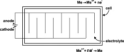
The scheme of an electrolytic cell for electrodeposition of metal powder is shown in the image. It is similar to a cell that is used for electroplating. The cell must have a slanting bottom so that the powder can be guided to a collection place for removal.

Image – Electrolytic cell for the deposition of metal powder.

This information is from ASM Handbooks Online, Vol. 5A: Thermal Spray Technology, Coating Structures, Properties, and Materials. To find this information (subscription required), click on the link below and scroll down to Figure 4.

https://dl.asminternational.org/handbooks/edited-volume/12/chapter/133823/Feedstock-Material-Considerations-for-Thermal


New ArcX center North America to be inaugurated in March

Höganäs, Sweden, is opening a new ArcX facility in Houston Texas to further strengthen the company’s position in the surface coating market and provide state-of-the-art technical support to its surface coating customers.

The 12,000 square foot facility will be located close to many big OEMs in various industries and will set global coating technology trends for the future. It will offer customer support, application development, technical solutions, as well as training, complimenting and building upon the other global ArcX centers within the Höganäs organization.

“Our new ArcX facility in the US is an important strategic move for Höganäs. Particularly in North America with many OEMs as driving forces to develop technological breakthroughs. This expansion is part of our company’s continued commitment to serving our customers in the Americas, helping us become a trusted technical partner for our customers and work together to create future opportunities,” says Hans Keller, President Surface & Joining Technologies.

Höganäs’ experts, who specialize in materials, processes, and customer applications, will make ArcX North America a unique development partner with full end-to-end knowledge; from concept development, prototyping, and process optimization to taking the products to the market. It will provide customers with the right material for the right application and the right process.

Selected capabilities:

Application development in laser, PTA and thermal spray

  • Pre-analysis on service condition and coating requirement
  • Concept creation, including material and process characterization
  • Prototyping
  • Coating test lab capabilities and full metallographic support

Process optimization for laser, PTA and thermal spray applications

  • Process/operational customer support
  • On-site troubleshooting and failure analysis
  • Provide in house or onsite training to help support customer’s growth needs


For more information:

Höganäs

https://www.hoganas.com/

Project looks at power of big data to predict hydropower component failures

Researchers from Argonne National Labs, Lemon, Ill., Idaho National Laboratories, Idaho Falls, Idaho, and Wayne State University, Detroit, Mich., are developing new models that can use data generated by sensors on hydropower components to predict how the components will degrade over time and estimate a component’s remaining life.
Digitally transforming risk prediction can guide effective operations and maintenance (O&M) policies for hydropower facilities, enabling proactive mitigation, reducing forced outages, and lowering O&M costs.

Researchers will leverage monitoring/sensor data from the Hydropower Research Institute, covering 44% of MW hydro-capacity in the U.S., and maintenance records and sensing data from industry partners.

Researchers will leverage hydro prognostics capabilities developed in Department of Energy Office of Energy Efficiency and Renewable Energy-Water Power Technologies Office (WPTO) seedling projects and integrate their asset management models into an open-source tool that will be co-developed with industry partners.

Feng Qiu, a principal computational scientist and group manager for advanced grid modeling – optimization and analytics at Argonne, is principal investigator for the project, which is funded with $500,000 from WPTO.


Image – Courtesy of: Shutterstock/DedMityay.


For more information:

Argonne National Laboratory

https://www.anl.gov/


Idaho National Laboratory

https://inl.gov/


Wayne State University

https://wayne.edu/


EAG Laboratories launches new NanoIR services

EAG Laboratories, San Diego, Calif., announced a new addition to its wide range of analytical techniques, NanoIR capabilities. NanoIR combines the nanometer scale spatial resolving capabilities of atomic force microscopy (AFM) with the chemical characterizing capabilities of infrared spectroscopy.

With this new capability, EAG scientists can provide clients with:

  • Simultaneous and correlative topographical, mechanical, and chemical information using a single tool
  • Spectroscopic characterization of trace materials such as surface contaminants and thin coatings with a spatial resolution down to ~10 nm (100x better than EAG’s best current Raman capabilities)
  • Complementary chemical information to existing microscopy and nanomechanical tools (AFM, SEM-EDS, TEM, NI, etc.)

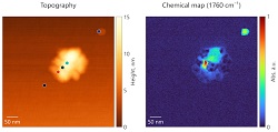
NanoIR spectra collected from the corresponding-colored locations indicated in the AFM image. Heterogeneities shown in the spectra are consistent with the chemical map, where the intensity of the PLGA ester peak (~1760 cm-1) varies across the particle and an additional ester species is detected (1730 cm-1).

Image – Data examples of PLGA nanoparticles deposited on mica. AFM height image (left) with colored markers indicating the corresponding analytical locations where spectra were obtained. A single wavenumber chemical map (right) taken at 1760 cm-1 reveals the ester-rich regions are detected only from the particles and are absent from the mica substrate. The chemical map highlights additional nanoscale heterogeneities that exist within the particles.


For more information:

EAG Laboratories

https://www.eag.com/

Exponent team receives DOE funds to advance EV battery technology

The DOE awarded $42 million in funding for 12 projects developing next-generation electric vehicle battery technologies to Exponent, Inc., Menlo Park, Calif., along with colleagues from the National Renewable Energy Laboratory (NREL) and the University of Texas, Austin. Project funding comes from the Department of Energy’s Electric Vehicles for American Low-Carbon Living (EVs4ALL) program.

“Exponent has been a leader in evaluating battery performance, risk, and safety for our clients for over 20 years,” said Ryan Spray, Ph.D., principal scientist at Exponent. “We look forward to the opportunity, with NREL and UT, to apply our deep expertise toward evaluating the energy storage technologies of tomorrow to enable new transportation possibilities.”

Deploying “clean” (zero emission) EVs is key to global decarbonization efforts. In the U.S., for instance, EVs4ALL reports that 80% adoption of EVs could reduce overall CO2 emissions by 800 million tons per year. However, the widespread adoption of EVs depends on developing more durable, faster-charging battery technologies that are effective at low temperatures.

Exponent’s team will focus on characterizing the risks posed by next-generation cells from fundamental reaction-kinetics of the materials all the way to the battery pack level. The project will lead the charge by investigating failure modes and effects, revising testing standards, and new capabilities and tools to help de-risk adoption of next-generation cells for commercial applications.


For more information:

Exponent, Inc.

https://www.exponent.com

Gatan introduces Cipher, the first tool to determine lithium content quantitatively in the scanning electron microscope

AMETEK Gatan, Inc., Berwyn, PA, a global leader focused on enhancing and extending the operation and productivity of electron microscopes, announced the launch of the Cipher system—the first and only system that reveals, quantitatively, the distribution of lithium in conventional scanning electron microscopes (SEM) and dual beam instruments.

To successfully reach the energy reduction pledges of governments worldwide, researchers are developing lithium compounds and alloys to improve the capacity and storage of renewable energy technologies. Quantifying and understanding the micro-scale distribution of lithium now becomes ever more pressing during the development of this integral technology. Still, the observation of lithium in bulk materials at these length scales has remained tantalizingly out of reach.

“For many years, a method to reliably detect lithium has been considered the ‘holy grail’ of microanalysis. However, due to fundamental limits of physics, reliable measurement of the lithium content in critical materials such as those used in lithium-ion batteries has proved unachievable,” says David Stowe, SEM Product Manager, Gatan/EDAX. “With the launch of Cipher, a ground-breaking method is now available to reveal the lithium content in metallic alloys, compounds, and complex metal oxides down to low single-digit weight percentages.”

Using an original concept, the Cipher system combines quantitative analysis of backscattered electrons and the x-ray fluorescence signal to reveal lithium using a composition-by-difference method. Building on AMETEK’s expertise in detector technologies, researchers can now utilize a turnkey solution in the DigitalMicrograph software to collect quantitative data, correlate, and analyze lithium at the micro-scale.

“With this release of the Cipher system, we see the accelerated innovation that was foreseen by bringing the EDAX and Gatan brands together,” commented Narayan Vishwanathan, vice president and business unit manager of AMETEK Electron Microscopy Technologies. “We now bring a reliable method to detect lithium that will fast-track the development of improved renewable energy materials.”

For more information:

AMETEK Gatan

https://www.gatan.com/

AI-designed chips reach scale with first 100 commercial tape-outs using Synopsys technology

Synopsys, Inc., Mountain View, Calif., reaches scale for AI-driven chip designs as major semiconductor customers register the first 100 commercial tape-outs with the company’s award-winning Synopsys DSO.ai autonomous design system. Recent customers, including STMicroelectronics and SK hynix, have all seen significant uplifts in productivity and PPA, and are now charting a new design course using reinforcement learning-enabled design tools on cloud and on-premise.

By using Synopsys DSO.ai (Design Space Optimization AI) the companies are setting a blistering pace for developing advanced-node chips through the key design phases. Customers experienced more than 3x productivity increases, up to 25% lower total power, and significant reduction in die size, with reduced use of overall resources.

Traditional design space exploration has been a highly labor-intensive effort, typically requiring months of experimentation. Using AI technology, Synopsys DSO.ai searches design spaces autonomously to discover optimal PPA solutions, massively scaling the exploration of choices in chip design workflows and automating many menial tasks.

“Delivering high-performance, robust memory products at industry-leading volumes demands intensive optimization, which has traditionally been highly human intensive,” said Junhyun Chun, head of SoC (System on Chip) at SK hynix. “Synopsys DSO.ai brings a huge amount of design team efficiency, giving our engineers more time to create differentiated features for our next generation of products. It’s also driving fantastic results as demonstrated in a recent project where DSO.ai delivered a 15% cell area reduction and a 5% die shrink.”

“AI’s ability to explore broader design spaces is accelerating our customers’ relentless drive towards better PPA and higher productivity with fewer engineering resources,” said Shankar Krishnamoorthy, GM for the EDA Group at Synopsys. “We’ve monitored the first 100 commercial tape-outs by customers using Synopsys DSO.ai and the results are compelling. Whether they’re designing in the cloud, on-premise or a hybrid of the two, it’s clear that in every case, designers are seeing significant gains from optimized designs delivering better results and faster time-to-market. The cloud-side is particularly exciting as deploying Synopsys AI technology at scale in data centers ushers an exciting new era for designers everywhere.”

“Microsoft is committed to democratizing advanced chip design, so it was a natural move for us to host the Synopsys DSO.ai design system on Azure,” said Jean Boufarhat, corporate vice president, engineering, Azure Hardware and Infrastructure at Microsoft. “With AI-powered chip design on Azure, companies can leverage cloud-scaling to boost productivity and optimize very large solution spaces like high-performance computing.”


For more information:

Synopsys, Inc.

www.synopsys.com

Veeco acquires Epiluvac AB to accelerate penetration into high growth silicon carbide epitaxy equipment market

Veeco Instruments Inc., Plainview, NY, acquired Epiluvac AB, Sweden, a privately held manufacturer of chemical vapor deposition (CVD) epitaxy systems that enable advanced silicon carbide (SiC) applications in the electric vehicle market. Epiluvac’s technology platform combined with Veeco’s global go-to-market capabilities create a significant long-term growth driver for Veeco.
The desire for clean, efficient, and reduced fossil-fuel energy is driving tremendous growth in the electric vehicle market. Applications such as on-board charging, fast charging and powertrain inverters are ideally suited for SiC power devices. The SiC device market is forecasted to grow approximately 30% compound annual growth rate (CAGR) from 2023 through 2027 according to Yole Group. Accordingly, the SiC epitaxy equipment market is expected to grow approximately 15% CAGR over the same time period according to Yole Group and internal Veeco estimates.

“The Epiluvac team has developed a superior platform and process know-how aligned with markets that are a great strategic fit for Veeco,” said Bill Miller, Veeco’s Chief Executive Officer.  “Their well-designed CVD platform achieves high productivity, is easy to maintain and has superior process control capability that make it uniquely qualified to produce devices that enable lighter, smaller and more efficient power conversion systems. We see this acquisition as a great complement to our metal organic chemical vapor deposition epitaxy product line. This acquisition accelerates our penetration into the emerging, high-growth SiC equipment market by reducing our time to market.”

“We are excited to join Veeco, a recognized leader in semiconductor and compound semiconductor capital equipment,” commented Per-Anders Eriksson, Epiluvac’s chief executive officer. “Our complementary technology platforms, along with Veeco’s extensive worldwide sales, service and manufacturing capabilities, will position us well to help our customers enable accelerated SiC adoption. The decades of research and development the Epiluvac team has invested in this demanding epitaxial process will be a great asset to Veeco’s already impressive process capabilities.”

Epiluvac is an early-stage revenue company with 11 employees. The purchase price for the transaction, all payable in cash, is $30 million paid at the time of closing with a potential additional $35 million in performance based earn-outs. The impact to Veeco’s financial results are not expected to be material in 2023 and volume revenue is expected to begin in 2024.


For more information:

Epiluvac AB

https://epiluvac.com/


Veeco

www.veeco.com


Award winning adaptive measurement templates speed up identification of deformed components

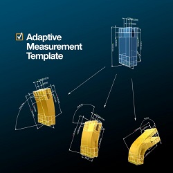
Leading software provider Volume Graphics, Germany, received a 2023 industry award for their Adaptive Measurement Template application that automatically compares original CAD intent against scan-based visualizations of parts, made with almost any material or manufacturing method, to assess quality and robustness. Volume Graphics’ Adaptive Measurement Templates has been named as one of the ten most innovative technologies for 2023 by a leading industry publication.
As CT scanning of parts becomes an increasingly routine quality-inspection step for manufacturers in automotive, aerospace, energy, medicine and other industries, the software that interprets that CT-scan data is becoming ever-more sophisticated, as well as more user-friendly.

An independent jury of machine-vision experts anonymously evaluated a shortlist of technology developments in image processing, metrology, embedded vision, and AI. The editorial team drew up the original list from around 30 products that stood out at trade fairs or in news articles over the past year. The jury then assigned points and selected the ten technologies with the highest total to be listed as Top Innovations. Products or solutions are selected because they enable more accurate, better, or simpler inspections for the industry.

Volume Graphics provides its Adaptive Measurement Templates in its latest versions of VGSTUDIO MAX, VGSTUDIO, VGMETROLOGY and VGinLINE software. These applications use data from CT-scanned objects to inspect and evaluate product quality. The shape-following templates speed up the identification of deformed components by allowing users to digitally apply metrics from their original CAD data or Product Manufacturing Information onto digital visualizations of the altered components, created from the CT scans.

The templates then highlight any differences between the original design and the as-manufactured-and-scanned part, and can be further applied to determine if such deviations are significant enough to affect performance or even cause rejection of the part.

This is highly valuable for the inspection of injection-molded parts and 3D-printed parts, which can often be out of tolerance and/or warped in such a way that a standard measurement plan, created on the nominal CAD object, cannot be applied easily or automatically to them. In such cases, correct analysis used to be possible only by applying time-consuming, local coordinate systems. The new Adaptive Measurement Templates apply dimensions and tolerances much more quickly, even to severely distorted parts, and can also inform design changes that improve final product quality.


For more information:

Volume Graphics

www.volumegraphics.com

Stacking LEDs instead of placing them side by side could enable fully immersive virtual reality displays

MIT engineers, Boston, Mass., have developed a new way to make sharper, defect-free displays, stacking the diodes to create vertical, multicolored pixels. Each stacked pixel can generate the full commercial range of colors and measures about 4 microns wide. The microscopic pixels, or micro-LEDs, can be packed to a density of 5,000 pixels per inch.

Over the years, the size of individual pixels has shrunk, enabling many more of them to be packed into devices to produce sharper, higher-resolution digital displays. But LEDs are reaching a limit to how small they can be while also performing effectively, especially noticeable in close-range displays such as augmented and virtual reality devices, where limited pixel density results in a “screen door effect” such that users perceive stripes in the space between pixels.

“This is the smallest micro-LED pixel, and the highest pixel density reported in the journals,” says Jeehwan Kim, associate professor of mechanical engineering at MIT. “We show that vertical pixellation is the way to go for higher-resolution displays in a smaller footprint.”

For next-generation displays, researchers are exploring inorganic micro-LEDs—diodes that are one-hundredth the size of conventional LEDs and are made from inorganic, single-crystalline semiconducting materials. Micro-LEDs could perform better, require less energy, and last longer than OLEDs.

Typical micro-LED fabrication using pick-and-place has required extreme accuracy, as microscopic pixels of red, green, and blue need to first be grown separately on wafers then precisely placed on a plate, in exact alignment with each other in order to properly reflect and produce various colors and shades. Achieving such microscopic precision is a difficult task, and entire devices need to be scrapped if pixels are found to be out of place.

The new MIT technique using vertical arrangement is an entirely different potentially less wasteful way to fabricate micro-LEDs.

The research group previously developed a method to grow and peel away perfect, two-dimensional, single-crystalline material from wafers of silicon and other surfaces—an approach they call 2D material-based layer transfer, or 2DLT.

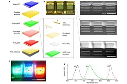
In the current study, this approach was used to grow ultrathin membranes of red, green, and blue LEDs. They then peeled the entire LED membranes away from their base wafers, and stacked them together to make a layer cake of red, green, and blue membranes. They could then carve the cake into patterns of tiny, vertical pixels, each as small as 4 microns wide.

“In conventional displays, each R, G, and B pixel is arranged laterally, which limits how small you can create each pixel,” Shin says. “Because we are stacking all three pixels vertically, in theory we could reduce the pixel area by a third.”

The team has shown that it can grow, peel, and stack ultrathin LEDs. As a demonstration, the team fabricated a vertical LED pixel, and showed that by altering the voltage applied to each of the pixel’s red, green, and blue membranes, they could produce various colors in a single pixel.

“If you have a higher current to red, and weaker to blue, the pixel would appear pink, and so on,” Shin says. “We’re able to create all the mixed colors, and our display can cover close to the commercial color space that’s available.”

The team plans to improve the operation of the vertical pixels. So far, they have shown they can stimulate an individual structure to produce the full spectrum of colors. They will work toward making an array of many vertical micro-LED pixels.

“You need a system to control 25 million LEDs separately,” Shin says. “Here, we’ve only partially demonstrated that. The active matrix operation is something we’ll need to further develop.”

Results are published in the journal Nature.


Image – Vertically stacked, full-color µLEDs enabled by 2DLT. Courtesy of: Nature (2023).  


For more information:

Massachusetts Institute of Technology

https://web.mit.edu/


Electronic bridge allows rapid energy sharing between semiconductors

Researchers at the Department of Energy’s Lawrence Berkeley National Laboratory (Berkeley Lab), Berkeley, Calif., discover that electrons play a surprising role in heat transfer between layers of semiconductors, with implications for next-generation electronic devices.

As semiconductor devices become ever smaller, researchers are exploring two-dimensional (2D) materials for potential applications in transistors and optoelectronics. Controlling the flow of electricity and heat through these materials is key to their functionality, but first we need to understand the details of those behaviors at atomic scales.

Curious about how electrons and atomic vibrations couple to one another when heat flows between two materials, zooming into the interface with atomic precision allowed the researchers to uncover a surprisingly efficient mechanism for their coupling.

“Our work shows that we need to go beyond the analogy of Lego blocks to understand stacks of disparate 2D materials, even though the layers aren’t strongly bonded to one another,” said Archana Raja, a scientist at Berkeley Lab at who led the study. “The seemingly distinct layers, in fact, communicate through shared electronic pathways, allowing us to access and eventually design properties that are greater than the sum of the parts.”

In stacked layers of the 2D semiconductor materials tungsten diselenide (WSe2) and tungsten disulfide (WS2), researchers found that although they aren’t tightly bonded to one another, electrons provide a bridge between them that facilitates rapid heat transfer.

The devices were fabricated by Raja’s group at Berkeley Lab’s Molecular Foundry, who perfected the art of using Scotch tape to lift off crystalline monolayers of the semiconductors, each less than a nanometer in thickness. Using polymer stamps aligned under a home-built stacking microscope, these layers were deposited on top of each other and precisely placed over a microscopic window to enable the transmission of electrons through the sample.

In experiments conducted at the Department of Energy’s SLAC National Accelerator Laboratory, the team used ultrafast electron diffraction (UED) to measure the temperatures of the individual layers while optically exciting electrons in just the WSe2 layer. The UED served as an “electron camera”, capturing the atom positions within each layer. By varying the time interval between the excitation and probing pulses by trillionths of a second, they could track the changing temperature of each layer independently, using theoretical simulations to convert the observed atomic movements into temperatures.

The UED approach enables a new way of directly measuring temperature within this complex heterostructure.  Aaron Lindenberg, a co-author on the study at Stanford University said “These layers are only a few angstroms apart, and yet we can selectively probe their response and, as a result of the time resolution, can probe at fundamental time scales how energy is shared between these structures in a new way.”

They found that the WSe2 layer heated up, as expected, but to their surprise, the WS2 layer also heated up in tandem, suggesting a rapid transfer of heat between layers. By contrast, when they didn’t excite electrons in the WSe2 and heated the heterostructure using a metal contact layer instead, the interface between WSe2 and WS2 transmitted heat very poorly, confirming previous reports.

“It was very surprising to see the two layers heat up almost simultaneously after photoexcitation and it motivated us to zero in on a deeper understanding of what was going on,” said Raja.

To understand their observations, the team employed theoretical calculations, using methods based on density functional theory to model how atoms and electrons behave in these systems with support from the Center for Computational Study of Excited-State Phenomena in Energy Materials (C2SEPEM), a DOE-funded Computational Materials Science Center at Berkeley Lab.

The researchers conducted extensive calculations of the electronic structure of layered 2D WSe2/WS2, as well as the behavior of lattice vibrations within the layers. Like squirrels traversing a forest canopy, who can run along paths defined by branches and occasionally jump between them, electrons in a material are limited to specific states and transitions (known as scattering), and knowledge of that electronic structure provides a guide to interpreting the experimental results.

Using computer simulations, the team explored where the electron in one layer initially wanted to scatter to, due to lattice vibrations. They found that electrons wanted to scatter to a hybrid state – a kind of ‘glue state’ where the electron hangs out in both layers at the same time. Now the team has a good idea of what these glue states look like and their signatures to confidently say that other, 2D semiconductor heterostructures will behave the same way.

The study appeared recently in Nature Nanotechnology.


Image – Artistic depiction of electron transfer driven by an ultrashort laser pulse across an interface between two atomically-thin materials. This transfer is facilitated by an interlayer ‘bridge’ state that electrons are able to access due to lattice vibrations in both materials. Courtesy of: Gregory M. Stewart/SLAC.


For more information:

Lawrence Berkeley National Laboratory

https://www.lbl.gov/

U.S. Department of Energy’s Office of Science

https://www.energy.gov/science/office-science

One Minute Mentor: Fluidized-bed heat treating furnace

The indirectly heated fluidized-bed furnace is heated electrically though a fluidized-bed furnace may also be gas heated. Fluidized beds have been designed to perform a wide variety of heat treating tasks including stress relieving, preheating, hardening, quenching, annealing, and tempering, as well as a variety of surface treatments such as carburizing, nitriding, and steam tempering.

Continue reading

How to grow a tiny metallic snowflake

Scientists at the University of Auckland, New Zealand, are working at the level of atoms to create something unexpected: tiny metallic snowflakes. During their research, they discovered that interactions between the atomistic structures of various metals and liquid gallium cause differently shaped crystals to emerge.

Continue reading

Microscopy and modeling help examine battery wear and tear

Researchers at the University of Chicago’s Pritzker School of Molecular Engineering (PME) have now used a combination of high-powered electron microscopy and computational modeling to understand exactly what occurs, on an atomic level, when lithium-ion batteries degrade. Their research points toward one approach to designing longer-lasting lithium-ion batteries—by focusing on the carbon binder domain (CBD).

Continue reading

Spray Tips: Powder production by sintering

Sintering refers to joining particles through the combined actions of pressure and heating. The pressed material is heated to below its melting point, and binding between particles occurs due to chemical diffusion between the particles. Further comminution and sieving is necessary to achieve the required particle size distribution. The fabrication of metal shapes from small particles by sintering is a 1000 year old technology. The sintering of metal and ceramics on a large scale is a more recent development that is mainly used for cermets, components made from a combination of metal and ceramics. The Co/WC class of materials are produced by these methods.

The image indicates that the individual particles become coherently joined in combination with some residual porosity during sintering. Porosity may be reduced by employing higher compaction pressures, higher sintering temperatures, and longer sintering times. However, such changes may be counterproductive in subsequent milling operations, because the strength of the product is greatly increased.

Sintered products normally involve processes that include powder production, shaping of the component from the powder, and strengthening of the powder agglomerate by heat treatment. The production of sintered powders can be considered a scaled-down version for producing engineered components.

Prior to sintering, components are heated to a temperature sufficient to evaporate any volatile components. Sintering is generally based on heating the green component to a temperature above the melting point of at least one of the powder constituents. The process must be completed in a reducing atmosphere or in a vacuum furnace.

It is first necessary to produce the powers of the appropriate chemistry that will be sintered into the desired feedstock. Powder production methods can be classified as either chemical or mechanical processes. The chemical routes include reduction, precipitation, chemical reaction, and electrolysis. The mechanical route includes atomization and disintegration. The reduction method produces powders from oxides of metals with high melting points. The most common reducing media are hydrogen and carbon. The reduced particles sinter together into a spongy mass that is crushed into a powder.

Large quantities of iron powders are produced using the carbon route. A typical precipitation method includes preparation of a carbonyl vapor by passing carbon monoxide at a high temperature over the heated metal. Precipitation of the vapor gives rise to a powder.

Powders are also produced by disintegration of a molten metal by a gas jet or water at high pressure (i.e., atomization). The key methods of producing powder are the atomization process and the reduction process.

Sintered powders exhibit agglomerated morphologies that are not spherical but can be described as being globular with many protuberances on the surface. It may be expected that such a powder is difficult to feed. This is generally true, but the thermal spray parameters for that particular material would be optimized, so these powders are technologically viable. A more important aspect is that the theoretical density of sintered powders is lower than powders obtained from the fused and crushed routes.

Because there is an empirical relationship that relates low densities to low tensile adhesion strengths, then agglomerated powders (or spray-dried and sintered powders) may exhibit lower strengths if their initial low density is reflected in the coating. It is emphasized that such powders are still acceptable for their intended applications and may have the additional benefit of being a lower-cost feedstock material.

The primary advantage of sintering for powder production is that it enhances particle strength so they retain their dimensions during transport to the TS source, as well as during their history within the intense thermal process zone. The sintering process results in some dimensional changes; however, these are not detrimental to the TS feedstock preparation because there will be a subsequent sieving operation.

Image – Sintering of particles.

This information is from ASM Handbooks Online, Vol. 5A: Thermal Spray Technology, Coating Structures, Properties, and Materials. To find this information (subscription required), click on the link below and scroll down to Figure 3.
https://dl.asminternational.org/handbooks/edited-volume/12/chapter/133823/Feedstock-Material-Considerations-for-Thermal


AMETEK Germany inaugurates new facility in Weiterstadt

Ametek Germany, part of Ametek Inc., inaugurated a new, state-of-the-art Customer Center of Excellence in Weiterstadt, Germany, that will provide enhanced support to its customers through in-person demonstrations of Ametek innovations and solutions across major industries.

The new facility features the latest products from numerous Ametek businesses, including SPECTRO, Taylor Hobson, Solartron Metrology, Creaform, MOCON, Reichert, Atlas, Brookfield, Zygo, Dunkermotoren, EGS, Motec, Powervar, SurgeX, Precitech and TMC. Service capabilities for Ametek products will also be provided.

Ametek Germany started its operations in 1973 in Meerbusch near Düsseldorf and continues to grow. In 2015, it opened the location in Weiterstadt, and since then, increasing customer demand has required an expansion to a larger facility. This new space will serve as an Ametek hub of innovation for numerous industries including aerospace & defense, automotive, food, pharma and packaging, high precision metrology, material analyses, oil and gas, and power.

It held a private grand opening event held in January where Ametek employees were on-hand to provide customers, distributors, and partners with dynamic and interactive technology demonstrations.

“We are thrilled to take this next step in expansion to solve our valued customers’ complex challenges using Ametek’s differentiated technology solutions,” said Wiebke Rumpf, Ametek Germany Country Manager. “This Customer Center of Excellence represents a significant milestone for Ametek’s operations in Germany, and its location near Frankfurt is perfect for customer events, distributor meetings, customer demos and much more.”


For more information:

AMETEK

www.Ametek.com


Powdermet wins the Weatherhead 100 Award

Powdermet, Inc., representing the entire PMT Group of companies, has again been named to the prestigious Weatherhead 100 list of the fastest growing companies in Northeast Ohio.

Established in 1988, the Weatherhead 100 Awards are the premier celebration of Northeast Ohio’s spirit of entrepreneurship and the companies that are leading the way in Northeast Ohio. Each year this program recognizes an elite group of companies that are the best example leadership, growth and success in Northeast Ohio. Companies that make the list earn this distinction based on their growth over the last five years.

Though Powdermet has been named to the Weatherhead 100 multiple times, this year they were recognized as the second-fasted growing organization on the list. Powdermet founder and CEO Andrew Sherman noted, “We’re very proud of this distinction and thankful to all our employees who made it possible. While our subsidiary Terves had an exceptional year, we had great performances from all PMT Group companies. This was an outstanding year and we’re poised for dramatic future growth with significant investment in both facilities and equipment being implemented in 2023.”

PMT group is excited to be part of reshoring and redeveloping critical materials manufacturing in the US. Apart from being the only integrated US wrought magnesium and part producer, PMT group companies are investing aggressively into increased production, rare earth metals, magnets, specialty alloys, and energy storage materials. PMT Group and its subsidiaries Terves, Magnesium USA, Powdermet, Hybrid Materials, Cratus, Magnet Energy and CermeTech are playing an important role in developing and commercializing critical solutions that will enable America to continue to lead and set the path for other nations to follow.


For more information:

PMT Group

https://www.tervesinc.com


The answer to why Roman concrete is so durable

Researchers have spent decades trying to figure out the secret of Rome’s ultradurable ancient construction material, used in the famed Pantheon as well as aqueducts and seawalls that endured especially harsh environmental conditions. Now, a team of investigators from MIT, Harvard University, and laboratories in Italy and Switzerland, has made progress in this field, discovering ancient concrete-manufacturing strategies that incorporated several key self-healing functionalities.
For many years, researchers have assumed that the key to the ancient concrete’s durability was based on one ingredient: pozzolanic material such as volcanic ash from the area of Pozzuoli, on the Bay of Naples. This specific kind of ash was even shipped all across the vast Roman empire to be used in construction, and was described as a key ingredient for concrete in accounts by architects and historians at the time.

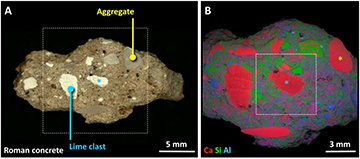
Under closer examination, these ancient samples also contain small, distinctive, millimeter-scale bright white mineral features, which have been long recognized as a ubiquitous component of Roman concretes. These white chunks, often referred to as “lime clasts,” originate from lime, another key component of the ancient concrete mix.

Upon further characterization of these lime clasts, using high-resolution multiscale imaging and chemical mapping techniques pioneered in Professor Admir Masic’s research lab at MIT, the researchers gained new insights into the potential functionality of these lime clasts.

Studying samples of this ancient concrete, he and his team determined that the white inclusions were made out of various forms of calcium carbonate. And spectroscopic examination provided clues that these had been formed at extreme temperatures, as would be expected from the exothermic reaction produced by using quicklime instead of, or in addition to, the slaked lime in the mixture. Hot mixing, the team has now concluded, was actually the key to the super-durable nature.

During the hot mixing process, the lime clasts develop a characteristically brittle nanoparticulate architecture, creating an easily fractured and reactive calcium source, which, as the team proposed, could provide a critical self-healing functionality. As soon as tiny cracks start to form within the concrete, they can preferentially travel through the high-surface-area lime clasts. This material can then react with water, creating a calcium-saturated solution, which can recrystallize as calcium carbonate and quickly fill the crack, or react with pozzolanic materials to further strengthen the composite material. These reactions take place spontaneously and therefore automatically heal the cracks before they spread. Previous support for this hypothesis was found through the examination of other Roman concrete samples that exhibited calcite-filled cracks.

To prove that this was indeed the mechanism responsible for the durability of the Roman concrete, the team produced samples of hot-mixed concrete that incorporated both ancient and modern formulations, deliberately cracked them, and then ran water through the cracks. Sure enough: Within two weeks the cracks had completely healed and the water could no longer flow. An identical chunk of concrete made without quicklime never healed, and the water just kept flowing through the sample. As a result of these successful tests, the team is working to commercialize this modified cement material.

Through the extended functional lifespan and the development of lighter-weight concrete forms, Masic hopes that these efforts could help reduce the environmental impact of cement production, which currently accounts for about 8% of global greenhouse gas emissions. Along with other new formulations, such as concrete that can actually absorb carbon dioxide from the air, another current research focus of the Masic lab, these improvements could help to reduce concrete’s global impact.

Image – Compositional and morphological characterization of ancient and modern lime clasts. (a) Optical micrographs showing the conspicuous bright white color of the lime clasts, which can easily be identified from large-area elemental mapping via SEM-EDS (b). Courtesy of Science Advances (2023). DOI: 10.1126/sciadv.add1602.

************

For more information:

Massachusetts Institute of Technology

Jabil strengthens additive manufacturing offerings

Jabil Inc. has launched PK 5000, an eco-friendly, powder-based additive material engineered to deliver improved strength, chemical resistance, and resilience in comparison to general-purpose nylon materials, such as PA 12. This patent-pending material has been formulated to support highly demanding automotive, consumer electronics, defense, medical, and industrial manufacturing applications.

PK 5000 was created, tested, and validated at Jabil’s Materials Innovation Center in Chaska, Minn., where polymer formulations, compound developments, and material system integration are completed from start-to-finish under one roof. Highly experienced additive manufacturing engineers, chemists, materials scientists, and production experts leverage Jabil’s innovations in materials science to oversee each step of the beaker-to-box process of developing customized powders and filaments all under an ISO 9001-2015 quality management system.

This newest material features a unique combination of chemical and mechanical properties, such as high-impact strength, high-abrasion resistance, and improved elongation over other nylon materials to withstand functional testing and use. Equally important, PK 5000 has high-barrier properties and low-moisture absorption, which may be critical for ensuring the quality and resilience of certain parts and products exposed to fuel and water. Moreover, the polyketone resin used to make PK 5000 is an eco-friendly, low-carbon material that is made from carbon monoxide. The ability to leverage carbon monoxide, which is a leading cause of atmospheric pollution, may reduce the overall carbon footprint.

In addition to advancements in materials, Jabil continues to extend its global additive manufacturing platforms and solutions to complement its world-class manufacturing capabilities. Jabil has deployed hundreds of 3D printers – from desktop models to highly sophisticated industrial systems – to address a vast range of prototyping, tooling and volume-scale production demands.

For more information: Jabil Inc.

https://www.jabil.com/

Engineers develop a new kind of shape-memory material

Massachusetts Institute of Technology, Boston, MA, has announced the discovery of a new category of shape-memory materials that could open up a new range of applications, especially for high-temperature settings, such as actuators inside a jet engine or a deep borehole.
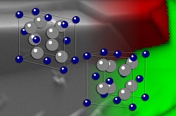
Shape-memory metals have long been used as simple actuators in a variety of devices but are limited by the achievable service temperatures of the metals used, usually a few hundred degrees Celsius at most. Ceramics can withstand much higher temperatures, sometimes up to thousands of degrees, but are known for their brittleness. Now, the MIT team has found a way to overcome that and produce a ceramic material that can actuate without accumulating damage, thus making it possible for it to function reliably as a shape-memory material through many cycles of use.


Read further here: https://news.mit.edu/2022/shape-memory-material-ceramic-1005


Surprising speed-dependent friction with graphene

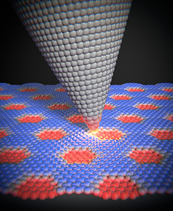
The speed at which an atomic force microscope moves across the surface of certain materials is influenced by the frictional properties of the substrate. One such example is graphene, which consists of a single layer of carbon atoms in a honeycomb arrangement. It is being examined with a view to potential use as a lubricating layer. Applications where a reduction of friction is desired include hard disks or moving components for satellites or space telescopes.

Previous studies have shown that a graphene ribbon can be moved across a gold surface with almost no friction. But if graphene is applied to a platinum surface, it has a significant impact on the measurable friction forces. Now, physicists from the University of Basel and Tel Aviv University have reported in the journal Nano Letters (“Velocity Dependence of Moiré Friction”) that, in this instance, the friction depends on the speed at which the tip of an atomic force microscope (AFM) is moved across the surface.

This finding is surprising because friction does not depend on speed according to Coulomb’s law, which applies in the macro world.

In conjunction with the platinum substrate, graphene no longer forms only the hexagonal honeycomb pattern of carbon atoms and instead forms superstructures known as Moiré superlattices. The surface is then no longer completely flat and exhibits a certain degree of roughness.

“If we move the AFM tip across this slightly corrugated surface at low speed, we measure a weak and almost constant frictional force,” explains Professor Ernst Meyer from the Swiss Nanoscience Institute and the Department of Physics at Basel University. “Above a certain threshold, however, the friction then increases with the speed of the AFM tip,” adds first author Dr. Yiming Song. “The larger the Moiré superstructure, the lower the threshold at which the friction becomes speed-dependent.”

The researchers found that there is greater resistance at the ridges of the Moiré superstructures during the movement of the tip. These ridges undergo elastic deformation due to the pushing tip before relaxing again when the pressure is sufficiently high. This effect results in greater frictional forces that increase with the speed of the tip. Simulations and an analytical model confirm the experimental findings obtained by this international team of researchers.

Image – The friction between the tip of an atomic force microscope and the Moiré superstructures depends on the speed at which the tip is moved across the surface. Courtesy of University of Basel.

************

For more information:

University of Basel