International Roadmap for Failure Analysis
The purpose of the International Roadmap for Failure Analysis is to leverage the technical expertise captured throughout the industry to identify both current and future FA challenges as part of an annual industry-wide gap analysis. To have this effort formalized and available across the industry in an interactive and inclusive manner will not only return a critical compilation of relevant action items it will also serve as a recognized technical platform from which future failure analysts will benefit. In addition, its purpose is to serve as a technical platform from which everyone connected to the industry can learn, interact, and prepare for the future.
IRFA Keynote
Monday, October 5, 2026 | 1:10 – 2:10 PM | Bridge Hall
Failure Analysis in the CMOS 2.0 Era: Navigating Disruptive Shifts and Technical Challenges
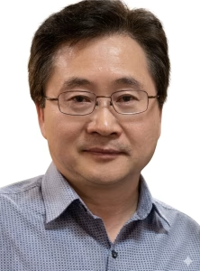
Dr. Zhiyong Ma, Intel
 Abstract: As classical 2D planar scaling reaches its physical and economic limits, the semiconductor industry has officially entered the CMOS 2.0 era. Defined by true 3D circuit-level disaggregation, this new paradigm shifts functional optimization into the vertical dimension through GAAFET/CFET architecture, Backside Power Delivery Networks (BSPDN), and high-density heterogeneous integration. While these innovations solve critical signal routing, IR drop, and power density bottlenecks, they fundamentally shatter traditional Failure Analysis (FA) and Fault Isolation (FI) eco-system, workflows and productivity. This keynote addresses three strategic pillars required to navigate the disruptive shifts and technical challenges to embrace accelerated AI-driven technology development cycles. First, we examine how aggressive scaling acts as a catalyst for pushing capability innovation, especially on defect isolation resolution, necessitated by the need to isolate defects buried within dense, multi-layer die stacks. Second, we analyze the disruption caused by Backside Power Delivery Networks (BSPDN) and 3D heterogeneous integration. By shielding traditional optical windows and burying critical interconnects, these technologies render decades of backside-probing methodology obsolete, driving the urgent development of probeless techniques and alternative defect isolation and detection ecosystems. Finally, we discuss the necessity of leveraging Artificial Intelligence (AI) to manage the massive data complexity and thermo-mechanical coupling inherent in heterogeneous systems. The report concludes that the future of reliability lies in a transition from die-level inspection to an AI-augmented, system-level diagnostic paradigm.
Biography: Dr. Zhiyong Ma is a distinguished industry leader with over 30 years of experience in semiconductor metrology, diagnostic capability, and technology development Q&R. Most recently, he served as Corporate Vice President and Director of Technology Development Quality & Reliability and the Foundry Q&R Lab Network at Intel. Throughout his career, Dr. Ma has championed strategic initiatives to advance lab metrology and debug ecosystems, directly supporting the progression of Moore’s Law through yield and reliability optimization. An accomplished scholar, he has co-authored over 40 technical papers and 2 book chapters on silicide technology and thin film kinetics, and served as lead editor of the book Metrology and Diagnostic Techniques for Nanoelectronics. Dr. Ma holds a PhD in Materials Science and Engineering from the University of Illinois at
Urbana-Champaign.
IRFA Session
Monday, October 5, 2026 | 2:10 – 3:45 PM | Bridge Hall
Session Schedule Breakdown:
10 min – IRFA Intro
Mr. Vinod Narang, Engineering Director, AMD, Singapore
The overview will cover IRFA’s vision, mission, organizational structure, key initiatives, and the 3-year cycle that identifies major industry FA gaps and drives solutions through coordinated working groups. It will also highlight current progress, member engagement, and opportunities to strengthen IRFA’s impact across the semiconductor ecosystem.
20 min – Die Level Fault Isolation
Dr. Venkat Ravikumar, Fellow, AMD, Singapore
Kristofor (Kris) Dickson, PMTS Advanced Silicon Pathfinding Team, AMD, Texas USA
As semiconductor technologies rapidly evolve toward stacked die architectures, backside power delivery, and sub-5nm nodes, traditional fault isolation techniques are reaching their limits. This session provides a unique look ahead at the challenges poised to reshape the future of failure analysis and the emerging solutions being developed to address them.
Attendees will gain insight into cutting-edge approaches including electron beam probing, circuit-level nanoprobing, X-ray assisted device alteration, magnetic field imaging, and AI-assisted diagnostics. The session will also explore the growing integration of failure analysis considerations into test and design flows, highlighting how the industry is adapting to increasingly complex product architectures.
Whether you work in failure analysis, design, product engineering, or test, this session offers a rare opportunity to understand where the field is heading, what new capabilities are emerging, and how these developments may impact your technical roadmap, tool investments, and problem-solving strategies in the years ahead.
20 min – Post Isolation
Mr. Nicholas Antoniou, FASM, Senior Product Manager, KLA Corporation, Milpitas, CA
Richard (Rick) Livengood, FASM, Principal Investigator / Intel Fellow (Retired), Si-FI Consulting, Glen Ellen, CA
The Post-isolation Domain Council covers 5 areas of Failure Analysis: Circuit Edit, Nanoprobing, Scanning Probe Microscopy, Sample Prep, and Microscopy. Gaps today, in the near-term future, and longer-term future will be presented and prioritized.
Circuit Edit is not only a design debug enabler but also allows for access to otherwise inaccessible parts of the circuit. Sample Prep is critical to most device analysis and Probing is critical to understanding chip performance.
Microscopy is used across the board and is indispensable for FA. Improvements in process and imaging resolution, throughput, automation, lack of standards and lack of formal training are common gaps across the different disciplines.
20 min – Package Innovation
Dr. Yan Li, Principal Engineer, Media Tek USA, San Jose, CA
Dr Peng Li, Senior Engineering Manager, Intel Corp. USA, Chandler, AZ
Advanced heterogeneous semiconductor packaging poses significant failure analysis (FA) challenges due to complex, multi-layered architectures and diverse defects. Isolating faults like micro-bumps and TSVs requires high-resolution, non-destructive techniques and precise physical FA (PFA), as traditional methods struggle with speed and precision. This presentation reviews recent advances in non-destructive imaging, PFA, and electrical FA. It highlights how AI-driven automation and multimodal data fusion are transforming defect detection workflows to overcome technical bottlenecks, while also addressing existing gaps and emerging future trends.
10 min – FA OC
Daminda Dahanayaka, Ph.D, MBA, Manager, Semiconductor Fab Operations, IBM Research
Keith Serrels, Failure Analysis Business Development/Strategic Account Manager, Hamamatsu Corporation
The FAOC has been chartered by the IRFA Leadership Team to improve the awareness of FA tools, techniques, and challenges across the broader semiconductor ecosystem. This has resulted in numerous formal engagements involving the Semiconductor Research Corporation (SRC), the IEEE, as well as several FA-adjacent workshops and conferences. This overview serves to offer a brief snapshot into these ongoing activities.
15 min – Q&A