Confluent Medical Technologies announces grand opening of Costa Rica expansion

Confluent Medical Technologies, Scottsdale, Ariz., has announced the grand opening of the latest addition to their large scale manufacturing center of excellence in Alajuela, Costa Rica, expanding their capacity for Nitinol processing and catheter manufacturing.

This new facility will be co-located with the existing Confluent Costa Rica facility and will add an additional 66,000 square feet to this location. The new site greatly expands Confluent’s capacity to process Nitinol components, as well as produce complex catheters using a combination of clean rooms and white-space manufacturing.

“Confluent has experienced consistent and strong growth in recent years,” said Confluent president & CEO, Dean Schauer. “This expansion supports our new product pipeline which continues to grow at a rate greater than Confluent has previously experienced.”

Confluent supports some of the fastest growing medical device markets such as interventional neurovascular, electrophysiology, structural heart, and peripheral vascular. As a result of the double-digit growth of these currently served markets, a substantial number of new products are coming into production and will utilize this new facility space immediately. Additionally, Confluent is considering additional expansion options beyond this new facility.

Read further here.

Furukawa Electric received the highest rating for CDP’s Supplier Engagement Rating for fourth consecutive year

Furukawa Electric, Tokyo, has received the top rating for its climate change initiatives across the entire supply chain and related information disclosure from CDP, an international environmental NGO. 

This is the fourth year in a row that Furukawa Electric has been recognized with this high rating, having been selected by CDP for its Leader of “A” rated companies. The Supplier Engagement Rating (SER) is an index that rates companies’ engagement with their supply chains concerning climate change issues and promotes coordination among companies in the value chain. Furukawa Electric has been acknowledged for its outstanding climate change initiatives, which are in line with the company’s goal of eliminating greenhouse gas emissions from its business activities (carbon neutral).

To achieve the sustainable development goals (SDGs) and realize Furukawa Electric Group Vision 2030, the company has been working on strengthening its ESG (Environment, Social, Governance) management. Furukawa Electric Group Environmental Vision 2050 was established in March 2021, declaring the company’s goal of achieving carbon neutrality. The company has also identified “Creating environmentally-friendly businesses” as a key management issue to be addressed to achieve Vision 2030 and is taking steps to enhance its responses to these materiality issues. Furukawa Electric’s commitment to environmental sustainability and its consistent recognition by CDP highlight the company’s ongoing efforts to lead the way in climate change initiatives and make a positive impact on the world.

Read further here. 

QMD precision components business now part of Cirtec Medical

Cirtec Medical Corp., Lowell, Mass., has acquired QMD Precision Components, a business that specializes in the development and manufacturing of silicone, polyisoprene, and other custom elastomeric components, tubing, and subassemblies. 

Cirtec is a strategic outsourcing partner of complex medical devices, including minimally invasive and active implantable devices. The acquisition will enable Cirtec to provide customers with advanced expertise in medical silicone molding and extrusion. The integration of Precision Components within the Cirtec brand will offer comprehensive, integrated solutions based on decades of silicone experience. The acquisition will also strengthen Cirtec’s platform for growth in existing markets such as active implantables, interventional, and minimally invasive surgical devices. Precision Components consists of Centers of Excellence in Sturtevant, Wisconsin, and Rock Hill, South Carolina, and engineering and manufacturing capabilities will remain at the facilities, along with current leadership.

Read further here. 


Neural network based control for magnetic shape memory alloy actuator

Sophia University, Japan, researchers have developed a new control scheme for the magnetic shape memory alloy-based actuator (MSMA-BA) that improves its positioning accuracy.

While MSMA-BA is a crucial component for high-precision positioning systems due to its high precision, low energy consumption, and large stroke, its hysteresis is an intrinsic property that can negatively affect its positioning accuracy. The team proposed a multi meta-model approach that combines the nonlinear auto-regressive moving average with exogenous inputs (NARMAX) and Bouc–Wen (BW) models to describe the dynamic hysteresis of MSMA-BA.

A wavelet neural network (WNN) was used to construct the nonlinear function of the multi meta-model, while iterative learning control was combined with a WNN to improve convergence speed. The proposed iterative learning controller was tested on MSMA-BA, with experiments demonstrating the scheme’s validity. The study’s main contribution was the convergence analysis of the iteration learning controller with iteration-dependent uncertainties.

Read further here.

Multi-furnace heat treat project for major steel forger

Nutec Bickley, Mexico, has been awarded a contract to manufacture and install five new lift-up furnaces, along with a fully modernized combustion system, for a leading U.S. manufacturer of high-quality alloy steel and carbon steel closed-die forgings. The project will take place between May and December 2023, with onsite work completed one furnace at a time to ensure the customer’s production schedules are not impacted. Two of the new furnaces will be used for tempering, while the remaining three will be used for austenitizing. Each furnace will be fitted with the latest control systems, complete fiber flues, and new exhaust and pressure control systems, along with insulation.

Nutec Bickley’s state-of-the-art combustion packages will be fully compliant with NFPA 86 standards, incorporating a fuel-only control system to allow maximum temperature uniformity potential for all cycles. The retrofitted furnaces will benefit from high-velocity nozzle mixing burners fitted with high-temperature burner blocks. The combustion systems will also feature automatic air control valves to adjust the maximum air volume used and to ensure proper burner ignition conditions.

The project will involve careful teamwork between the customer and Nutec Bickley to ensure successful delivery and highest quality outcomes. Rodrigo González, VP Metals at Nutec Bickley, emphasized the importance of constant communication and status updates with customers for a dynamic and mutually beneficial project result.


Read further here

One Minute Mentor: Continuous Operating Furnaces for Tool Steel Strips

The continuous heat treatment of tool steel is applied to low- or medium-alloyed carbon steel strips as well as martensitic stainless steels. The described lines produce high-quality strip with respect to uniform structure, flatness, and bright surface finish. Steel grades with 0.4 to 1.2% C, low and high alloyed, can be processed. Strip dimensions range between 10 to 750 mm (0.4 to 29.5 in.) wide and 0.05 to 4 mm (0.002 to 0.16 in.) thick. High quenching rates are necessary, especially for plain carbon steels. Cooling gradients of up to 600 K/s are possible in a molten lead-bismuth quench. Because two-stage quenching technology provides considerable advantages over quenching in oil, this method has been adopted worldwide. It is also possible to achieve isothermal transformation to bainite and pearlite using a molten metal quench, so this type of hardening and tempering line is extremely versatile.

The configuration of a high-performance line involves an entry and exit section of the strip handling equipment (Fig. 10). The hardening section consists of the austenitizing furnace, the molten metal quench or hydrogen quench, and a martensite cooler. Beyond the martensite cooler the strip is martensitic and fully hardened, and then it passes through the tempering section—consisting of a leveling furnace, tempering furnace equipped with an atmosphere recirculation system, and an atmosphere jet cooler—to finally leave the facility, completely flat, with a bright surface finish and tempered to very uniform tensile strength.

For more information, click on the link below (subscription required). Then scroll to Figure 10

R Schneider ; R. Mesquita ; H. Altena ; T. Müller ; P. Seemann,Processes and Furnace Equipment for Heat Treating of Tool Steels, ASM International, 2014, https://doi.org/10.31399/asm.hb.v04d.a0005958

Wisconsin oven ships pin conveyor oven to automotive manufacturer

Wisconsin Oven Corp., East Troy, has shipped one electrically heated conveyor oven to an automotive manufacturer, which will be used for tempering automotive parts. The conveyor oven features a chain style conveyor system with vertical pins, ensuring the uniform transfer of parts through the heating and cooldown zones of the oven. The maximum temperature rating of the conveyor oven is 260° C, with interior chamber dimensions of 3’6” W x 20’10” L x 9” H.

The conveyor oven also features a top-down bottom-up airflow configuration designed with a 55,000 CFM @ 50 HP blower, ensuring optimal temperature uniformity of ±2.5° C at 163°C, documented with a temperature uniformity test. The oven is equipped with a continuous chain conveyor with vertical pins, programmable temperature controller, and recorder with Ethernet capabilities.

The unique features of this tempering oven include the ability to automatically scan the parts while being loaded onto the conveyor and validate that the correct part is being loaded, providing a pass/fail regarding heating time and temperature. The conveyor oven also includes an ambient cooldown zone and supervised installation with start-up and training.

Mike Grande, vice president of sales,said that, “Our continuous designs provide customers with innovative solutions to meet their load and process requirements. This conveyor oven was designed with high-velocity impingement air nozzles for rapid, uniform heating and optimal part results.” The equipment was fully factory tested and adjusted prior to shipment from the facility, ensuring it met all Wisconsin Oven quality standards. The equipment comes with a 2-year warranty, providing peace of mind for the automotive manufacturer.

Read further here.

Ipsen repurposes ceramics facility for expanded hot zone production capacity

Ipsen, Pecatonica, Ill., formerly known as Ipsen Ceramics, is expanding its vacuum furnace hot zone assembly. The refurbishments include new lighting, HVAC, roofing, and other interior and exterior upgrades. Located at 325 John Street, less than 30 miles from Ipsen’s Vacuum Technology Excellence Center in Cherry Valley, the factory will initially employ up to eight material assemblers.

Incorporating the Pecatonica location into Ipsen’s vacuum furnace production and aftermarket process will provide added benefits to customers. Jake Hamid, Ipsen’s director and chief Operating Officer, stated that “Our goal is to reduce delivery times and better control the critical phase of assembly.” In the future, Ipsen is considering other manufacturing activities in Pecatonica to supplement the needs of the Vacuum Technology Excellence Center.

The move to repurpose the Pecatonica plant aligns with Ipsen’s commitment to providing high-quality vacuum furnace equipment and services to customers. The company’s dedication to meeting customer needs and reducing delivery times will be further enhanced by this strategic move, ensuring that Ipsen remains a leader in the vacuum furnace industry.

Read further here.

Leading die manufacturer adds Seco/Vacuum furnace to increase capacity

Seco/Vacuum, Meadville, Pa., has announced that a U.S.-based international manufacturer has placed an order for a Vector high-pressure gas quench furnace. The new furnace will increase the partner’s heat treat capability while improving part quality. The Vector will allow the partner to heat treat larger parts, at higher quantities per cycle than their existing furnace, all with improved quality control and reliability.

The partner’s equipment requires the use of large dies that require precise heat treating. Their current heat treatment setup includes a pair of vacuum furnaces, which have some limits compared to the Vector they are about to receive.

The new furnace, a bottom loading Vector vacuum furnace with 6 bar nitrogen gas quench, has a 60″ diameter, 72″ tall, and a 3-ton capacity working zone. It is equipped with convection heating which allows them to run their tempering cycle in the same furnace without having to move parts after hardening, a tremendous time and labor savings.

The furnace is also equipped with SECO/WARWICK’s FineCarb low-pressure carburizing system for future process developments. The Vector will increase production capacity to meet the rising market demand of today and tomorrow. The new furnace’s vertical configuration and rotary hearth were built specifically to accommodate more large dies, allowing the partner to meet the elevated demand with ease. SECO/VACUUM’s intuitive process controls ensure greater heating uniformity than their existing equipment in both convection mode and in vacuum mode.

Read further here

Mysteries of atomically thin mica resolved

Mica, a common mineral found in granite, and has been extensively studied from geological, chemical, and technical perspectives. But recently a team from the Vienna University of Technology presented a study that explains the distribution of potassium ions on the mica surface. The researchers used a new type of atomic force microscope to conduct their investigation. Prior to this, the physical surface details of mica have never been studied on an atomic scale.

Continue reading

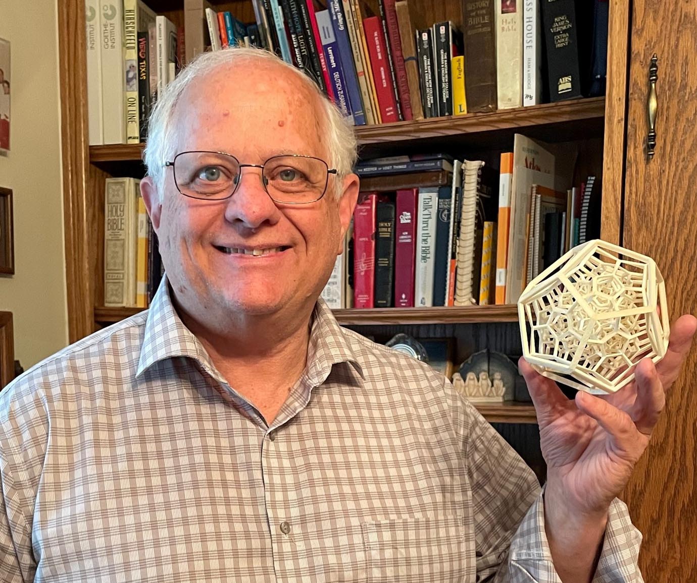
Contributor Corner: David L. Bourell, Ph.D., FASM

Dr. David L. Bourell recently retired from The University of Texas at Austin, where he was the Temple Foundation Professor Emeritus and served for 43 years as a professor in the Walker School of Mechanical Engineering, and in the Materials Science and Engineering Graduate Program.

Dr. Bourell, a Fellow of ASM International (FASM), has always placed a high premium on ASM International Handbook development. He co-authored his first ASM Handbook article 25 years ago for ASM Handbook, Volume 7: Powder Metallurgy (1998 edition) and ASM Handbook, Volume 20: Materials Selection and Design (1997). Most recently, Dr. Bourell was a co-Volume Editor of the upcoming ASM Handbook, Volume 24A: Additive Manufacturing Design and Applications (scheduled to publish later in 2023). He also served as co-Volume Editor and authored several articles for ASM Handbook, Volume 24: Additive Manufacturing Processes (2020).

One of Dr. Bourell’s most appreciated awards was the 1986 ASM International Bradley Stoughton Award for Early Career Teachers. Later in his career, in 1999, he was awarded the University of Texas College of Engineering Lockheed Martin Award for Excellence in Engineering Teaching (awarded annually to one person from the 270-member faculty.)

Dr. Bourell is a pioneer in additive manufacturing (AM), and was one of the first materials researchers to enter this field. He developed advanced material systems for Laser Sintering (LS), a powder bed fusion process, having worked in this area since 1988. According to the Wohlers Report, polyamide feedstock for this process is the most popular AM material among commercial users. He was the lead author on the first materials patent for LS technology. Issuing in 1990, this patent has been cited by 315 other patents. He holds 10 primary patents and has published 290 papers. Dr. Bourell was the first person to use a modern AM fabricator to produce a fully metal part (1990).

Service has been a hallmark of Dr. Bourell’s career. He has advanced the field of AM in various ways. He was a founding member of the organizing committee for the Annual International SFF Symposium — an Additive Manufacturing Conference (1990), chairing this group from 1995 to 2022. (The SFF Symposium is the longest running, premier research conference on AM in the world.) Dr. Bourell is a founding member of the ASTM F42 Technical Committee on Additive Manufacturing and currently serves on the F42 Executive Committee and the ten-member ASTM/ISO Joint Group 51 on Terminology for AM. He recently received that organization’s Frank W. Reinhart Award for “outstanding and unusual contributions to the organization in the realm of terminology standardization” (2022).

Dr. Bourell is also active in and a fellow of The Minerals, Metals, and Materials Society (TMS), serving on numerous technical committees and the Society’s Board of Directors. In 2017, he received the Society of Manufacturing Engineers Albert M. Sargent Progress Award for “significant accomplishments in the field of manufacturing processes.” He was the 2011 recipient of the SFF Symposium Freeform and Additive Manufacturing Excellence (FAME) Award. In recognition of his service to the profession, he was the 2012 Recipient of the University of Texas Cockrell School of Engineering Joe J. King Professional Engineering Achievement Award, given to a single member of the 270-member faculty.

For over 25 years, Dr. Bourell has served as a member and officer of the technical committee that writes the Principals and Practice exam for Materials and Metallurgy, used by many states as part of the professional engineering registration process (he currently chairs this committee). He also enjoys writing tests for use in the Texas high school STEM competition on Calculator Applications, which is the pre-engineering test given under the aegis of the University Interscholastic League; more than 4,000 high-school students compete in this event annually. He started as a co-director of the contest in 1982, and he has directed it since 1997.

Dr. Bourell enjoys playing bass guitar, and owns a 3D-printed electric bass guitar. He also enjoys traveling, having traveled 2.7 million miles and visited over 30 countries on six continents.

TZ6000 – a nondestructive wafer quality measurement tool for the compound semiconductor industry

ACE Solution, Taiwan, the leader and the provider in customized test solutions to meet customer needs in electrical components, devices and system manufactures, launched the TZ6000 – a nondestructive wafer quality measurement tool for the compound semiconductor industry. Incorporated with TeraPulse Lx technologies from TeraView, United Kingdom, the TZ6000 achieves nondestructive wafer quality measurements of thickness, refractive index, resistivity, dielectric constant, surface/subsurface defects at selected positions and whole wafer scanning map.

Dr. JC Chen, VP of R&D of ACE Solution, commented “The quality of the semiconductor wafer determines the maximum achievable conversion efficiency to the final device. Subsurface damages (SSD) of semiconductor wafers are easily induced during surface machining process includes rough grinding, fine grinding, and chemical mechanical polishing. Current wafer inspection systems which rely on VIS/IR/UV optical inspection can analysis the surface properties of the wafer but not the SSD, due to their low penetration depth. Terahertz (THz) wave has higher penetration depth in semiconductor wafers as silicon, silicon carbide and gallium nitride. We developed the THz-based TZ6000 to meet the market need of nondestructive inspection of the compound semiconductor wafer.”

Dr. Philip F. Taday, head of applications and principal scientist of TeraView, commented “The TeraPulse Lx system is TeraView’s world-leading product family for terahertz analysis. It has been designed to meet the needs of the material inspection in imaging or spectroscopy applications, and is ideal for compound semiconductors. The system’s modular architecture and TeraView patented laser-gated photoconductive emitters and detectors gives the user both flexibility and expandability. The system also boasts an industry-leading 3,200 ps time-delay line, as standard.”

Steve Hsu, CEO of ACE Solution, commented “ACE Solution is the leading company in providing electrical precision test, integrating service and solution. It is great opportunity to collaborate with TeraView and incorporate the TeraPulse Lx module into TZ6000 system for nondestructive wafer quality inspection. TZ6000 has high flexibilities for various sizes and forms of wafers. It is provided with TeraView’s unique THz-TDS probe for simultaneous measurement of multiple parameters of wafer characterization. TZ 6000 has a user-friendly and graphic illustrate software for quality inspection in wafer manufacturing process and R&D.”

Dr. Don Arnone, CEO of TeraView, commented “This is another first from TeraView to have a close collaboration with ACE Solution to develop this product, and we are quite confident that this product will set a new standard in compound semiconductor wafer quality analysis and defect inspection. The TeraPulse Lx system is designed with a lightweight compact core unit which allows for easy transport between locations. Incorporated with TeraView’s TeraPulse Lx modules, we can address the growing needs of the compound semiconductor wafer industry with this product.”

Image – Left: TZ6000 System incorporated with TeraPulse Lx; Middle: Steve Hsu, CEO of ACE Solution. Right: Dr. Philip Taday, Head of Application of TeraView.

For more information:

ACE Solution, Co., Ltd.

https://www.acesolution.com.tw/en/index/

TeraView

https://teraview.com/

FormFactor opens Silicon Valley Demo Center

FormFactor, Inc., Livermore, Calif., a leading semiconductor test and measurement supplier, opened a new product demonstration and training center in San Jose, California. The facility is staffed with applications engineers and training professionals, and features

FormFactor engineering wafer probers, metrology systems and advanced probe cards outfitted to meet semiconductor test and measurement requirements from lab to fab, including solutions for advanced packaging, automotive high-power devices, high-speed digital, silicon photonics, and 5G/6G/millimeter-wave mobile devices.

“The opening of our new demonstration center provides easy access for our customers to see first-hand the benefits of our sophisticated wafer probe and metrology solutions,” said Amy Leong, senior vice president and chief commercial officer. “We are deeply committed to enabling industry innovation, and proud to offer this center to accelerate our customers’ success with personalized, hands-on training, product demonstration, and support.”

FormFactor’s new demonstration center is located in the heart of Silicon Valley and offers a product demonstration lab and clean room, presentation and training areas, service warehouse, office space and conference rooms. The new location complements the capabilities of FormFactor’s existing global demonstration centers in Europe and Asia, and recently opened Advanced Quantum Cryogenic Lab in Boulder, Colorado.
For more information:

FormFactor, Inc.

www.formfactor.com

JEOL introduces new FIB-SEM for fast, atomic resolution STEM sample preparation

JEOL, Peabody, Mass., developed a new Focused Ion Beam (FIB) solution for preparing specimens prior to observing them in the Transmission Electron Microscope (TEM). The new JIB-PS500i is a multipurpose FIB-SEM that delivers the synergy of fast sample preparation, SEM imaging and EDS analysis in a single instrument.

The new FIB sample stage offers fast transitioning between processing and imaging, allowing for real-time feedback of specimen quality. With the ability to prepare samples thinner than 30nm, the FIB-SEM produces a sample suitable for superior atomic resolution imaging and analysis with STEM (Scanning Transmission Electron Microscope). A retractable STEM detector enables easy acquisition of bright field and dark field images during processing to precisely evaluate preparation of the TEM sample. The operator can easily prepare TEM specimens using the STEMPLING2 automatic TEM specimen preparation system, which allows unattended preparation of multiple samples.

A specially designed double-tilt sample holder, TEM-Linkage, enables seamless transfer from the FIB-SEM directly to the TEM.

A key advantage of the JIB-PS500i FIB is the large specimen chamber with an easy-access door. This design supports an efficient workflow and flexibility for a variety of samples and processes. The 5-axis full-eucentric large motor stage is designed to transport both large and multiple samples in the XY direction, and at a wide stage tilt and rotation range.

A new high current (up to 100 nA) FIB column is especially effective for large-area processing and analysis, which is ideal for semiconductor samples. The new FIB has high performance fine milling capabilities essential for quality lamella preparation imaging, EDS analysis, and 3D microscopy. The new JIB-PS500i has superior performance in the low kV range, as low as 0.5kV, essential for beam sensitive materials.


For more information:

JEOL USA, Inc.

https://www.jeolusa.com/

Perovskites, a ‘dirt cheap’ alternative to silicon, just got a lot more efficient

A study at the University of Rochester, Rochester, N.Y., suggests perovskites — a family of materials nicknamed for their crystalline structure that have shown extraordinary promise in recent years as a far less expensive, equally efficient replacement for silicon in solar cells and detectors — may become far more efficient.

Researchers typically synthesize perovskites in a wet lab, and then apply the material as a film on a glass substrate and explore various applications. Chunlei Guo, professor of optics at the University of Rochester leading the study reported in Nature Photonics, instead proposes a novel, physics-based approach.

By using a substrate of either a layer of metal or alternating layers of metal and dielectric material—rather than glass—he and his coauthors found they could increase the perovskite’s light conversion efficiency by 250 percent.

“No one else has come to this observation in perovskites,” Guo says. “All of a sudden, we can put a metal platform under a perovskite, utterly changing the interaction of the electrons within the perovskite. Thus, we use a physical method to engineer that interaction.”

Metals are probably the simplest materials in nature, but they can be made to acquire complex functions. The Guo Lab has extensive experience in this direction. The lab has pioneered a range of technologies transforming simple metals to pitch black, superhydrophilic (water-attracting), or superhydrophobic (water-repellent). The enhanced metals have been used for solar energy absorption and water purification in their recent studies.

In this new paper, instead of presenting a way to enhance the metal itself, the Guo Lab demonstrates how to use the metal to enhance the efficiency of pervoskites.

“A piece of metal can do just as much work as complex chemical engineering in a wet lab,” says Guo, adding that the new research may be particularly useful for future solar energy harvesting.”

In a solar cell, photons from sunlight need to interact with and excite electrons, causing the electrons to leave their atomic cores and generating an electrical current, Guo explains. Ideally, the solar cell would use materials that are weak to pull the excited electrons back to the atomic cores and stop the electrical current.

Guo’s lab demonstrated that such recombination could be substantially prevented by combining a perovskite material with either a layer of metal or a metamaterial substrate consisting of alternating layers of silver, a noble metal, and aluminum oxide, a dielectric.
The result was a significant reduction of electron recombination through “a lot of surprising physics,” Guo says. In effect, the metal layer serves as a mirror, which creates reversed images of electron-hole pairs, weakening the ability of the electrons to recombine with the holes.

The lab was able to use a simple detector to observe the resulting 250 percent increase in efficiency of light conversion.
Several challenges must be resolved before perovskites become practical for applications, especially their tendency to degrade relatively quickly. Currently, researchers are racing to find new, more stable perovskite materials.

“As new perovskites emerge, we can then use our physics-based method to further enhance their performance,” Guo says.


Image – This illustration from the Guo Lab shows the interaction between a perovskite material (cyan) and a substrate of metal-dielectric material. The red and blue pairings are electron-hole pairs. Mirror images reflected from the substrate reduce the ability of excited electrons in the perovskite to recombine with their atomic cores, increasing the efficiency of the perovskite to harvest solar light. Courtesy of: Chloe Zhang.


For more information:

University of Rochester

https://www.rochester.edu/

Argonne scientists develop new X-ray data reconstruction method

Scientists at the Argonne National Laboratory Advanced Photon Source (APS), Lemont, Ill., are exploring ways to analyze X-ray data faster and with more precision; its new TomocuPy software package has shown to be up to 30 times faster than the current practice.
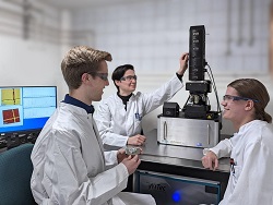
Collecting and processing X-ray data faster is especially important for scientists working at the APS, which is about to undergo an extensive upgrade increasing the brightness of its X-ray beams by up to 500 times. Scientists use those beams to see ions moving inside batteries, for instance, or to determine the exact protein structure of infectious diseases. When the upgraded APS emerges in 2024, they will be able to collect that data at an exponentially faster rate.

To keep pace with the science, the analysis and reconstruction of that data — which shapes it into a useful form — will also have to get much faster before the APS Upgrade is complete. Argonne scientists have been working on multiple new methods using artificial intelligence to help speed up the timeline. Faster processes have been created for X-ray imaging and for determining important data peaks in X-ray diffraction data, to name a couple.

Argonne’s Viktor Nikitin, an assistant physicist working at the APS, has now unveiled a new way of reconstructing data taken through a process called tomography. Nikitin’s software package, called TomocuPy, builds on the current tools scientists use for tomography data. It improves the speed of the process by 20 to 30 times by leveraging computers equipped with graphics processing units (GPUs) and by reconstructing several chunks of data at once.

Nikitin’s innovations are important, and they involve an understanding of how tomography works: slice by slice. Tomography involves using an X-ray beam to observe multiple parts of the sample, extracting cross sections (or slices) from them, and then using a computer to reconstruct those slices into a whole. Nikitin’s TomocuPy builds a pipeline for processing those slices where the sequence of operations, such as reading and writing from hard disks and computations, can happen concurrently. Current methods examine each slice one at a time and put them together on the back end.

TomocuPy also takes advantage of the multiple processors within each GPU being used, and runs them all simultaneously. Stack up enough of these, and thousands of slices can be viewed in the time it would previously have taken to analyze one. Nikitin’s method also saves computing time by lowering the analysis precision of each GPU to match the output from the detector — if the output is 16-bit, he says, you don’t need 32-bit calculations to analyze it.

“Tomography is a lot of small operations, processing small images,” Nikitin said. “GPUs can do it up to 30 times faster. The previous method uses CPUs and doesn’t use the information pipeline that TomocuPy does, and it’s far slower.”

The GPUs in use for TomocuPy are often used for artificial intelligence applications, and can be adapted to work with machine learning algorithms. This is important, Nikitin said, because the eventual goal is experiments that can adjust to reconstructed data in real time.

Eventually, Nikitin said, the plan is to use artificial intelligence to help direct experiments, either by automatically zooming in on the interesting parts of a sample, or changing the environmental conditions like temperature and pressure in response to quickly reconstructed huge amount of APS Upgrade data. This will be possible, he said, with help from the massive supercomputers at the Argonne Leadership Computing Facility.

“We are building a fast connection between APS and ALCF,” he said. “By running TomocuPy on a supercomputer, we can do in a day what now can take up to a month.”

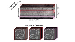
Image – TomocuPy allows for processing chunks of data concurrently in real time, making the entire reconstruction process faster. It moves chunks of data between processing units and returns the analyzed data to the storage drive much more quickly than current methods. Courtesy of: Viktor Nikitin/Argonne National Laboratory.


For more information:

Argonne National Laboratory

https://www.anl.gov/

Raman microscope at the forefront of battery research

WITec GmbH, the originator of commercial Raman imaging systems, has delivered a new alpha300 R instrument to the Center for Solar Energy and Hydrogen Research (ZSW) Baden-Württemberg in Ulm, Germany. The Raman microscope will be used in the “Powder-Up!” pilot plant in Ulm, where cathode materials for lithium-ion batteries will be produced and the scalability of fabrication methods will be investigated.

Lithium-ion batteries are the primary enabling technology in the current shift toward electric mobility and their performance is almost exclusively determined by the materials used. ZSW is at the forefront of innovative energy storage development and is constructing a new building for the “Powder-Up!” pilot plant over the next twelve months. The new facility will focus on making improvements in the next generation of battery electrode materials, and on scaling up their manufacturing processes. This work is set to have far-reaching effects in terms of battery performance, resource use, and unit costs.

According to Dr. Margret Wohlfahrt-Mehrens, head of the Accumulators Materials Research department, “Raman microscopy is becoming a standard method in applied battery research. It quickly provides detailed information about how different electrode formulations function and degrade over charge cycles.”

WITec GmbH won the Europe-wide public tender due to the high chemical sensitivity, spatial resolution and acquisition speed of its Raman imaging systems. The alpha300 R microscope offers the added benefits of modularity for integrating hardware such as electro-chemical cells, and high sample throughput for compiling industrially relevant volumes of data.

The “Powder-Up!” facility, funded by the Baden-Württemberg Ministry of Economic Affairs, Labor and Tourism and the German Federal Ministry of Education and Research (BMBF), is the first of its kind in Europe. Material batches of up to 100 kilograms can be produced in the new plant. Such quantities are required to produce large battery cells for electric cars or stationary energy storage units.


Image – Florian Klein (left) and Leon Gläser (right) from the ZSW in Ulm together with WITec Application Scientist Dr. Ievgeniia Iermak (middle) during training on the new Raman microscope.


For more information:

Oxford Instruments Group

https://www.oxinst.com

The Center for Solar Energy and Hydrogen Research Baden-Württemberg

https://www.zsw-bw.de/en.html

Rome wasn’t built in a day, but they sure had strong concrete

The Roman Colosseum is a giant, oval amphitheater built almost two thousand years ago. Despite its age and a 14th century earthquake that knocked down the south side of the colosseum, most of the 150-some foot building is still standing. Like many ancient Roman structures, parts of it were constructed using a specific type of concrete. Scientists and engineers have long suspected a key to these buildings’ durability is their use of this Roman concrete. But exactly how this sturdy concrete has contributed to the architecture’s strength has been a mystery to researchers across the globe.
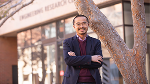
A team of interdisciplinary researchers recently discovered a potential answer to why these ancient Roman buildings have been able to weather the test of time while many modern, concrete structures seem to crumble after a few decades.

The answer: self-healing concrete.

The material has three components: limestone, volcanic material and water. For years, architects and historians have speculated the volcanic material is what makes it strong — which it does. But it does not explain the material’s self-healing ability.

What the researchers found was that the self-healing properties might simply be a serendipitous manipulation of chemistry. The limestone in the concrete is likely the secret.

When the ancient Romans made mortar, they heated up the lime to turn it into a substance called “quicklime” – a very reactive chemical sibling to limestone. And, because they introduced water to the quicklime during mixing, the heat it produced set up a chemical foundation that could strengthen the concrete later.

When tiny cracks start to form later, the quicklime stops them from becoming bigger. When it rains, the lime reacts with the water to recrystallize as various forms of calcium carbonate, quickly filling the crack or reacting with volcanic ash to “heal” the material.

For materials scientist Ainissa Ramirez, this new understanding of ancient Roman concrete is a welcome discovery.

“This is one way that the material can be greener,” says Ramirez. “It’s sort of like a message in a bottle. The Romans made the material. We had to kind of figure out how they did it so that we can make better materials — and then, you know, in turn, be better stewards of our environment.”

For more information: Science Advances 

When quantum computing meets alloy design

Although research alloy design and artificial intelligence has been ongoing for decades, Houlong Zhuang is now combining the two fields to forge a new path forward for materials scientists.

Zhuang’s vision is quickly gaining traction. In fact, the first research article he published about incorporating the use of artificial intelligence to design alloys has already been cited nearly 250 times since 2019.

The National Science Foundation, or NSF, grants the Faculty Early Career Development Program, or CAREER, award to early-career faculty members who have the potential to serve as academic role models in research and education and to lead advances in the mission of their department or organization.

Zhuang has been awarded a $537,000 CAREER award from the NSF to pursue this research in alloy design and quantum computing in his project “Developing Quantum Algorithms for High-Entropy Alloy Discovery.”

Alloy design involves the development of materials made with various metals blended together to create an ideal structural composition. Quantum computing operates by using the subatomic particles in physical matter to store information, then leverages this behavior using specialized hardware. The data drawn from quantum computing can be used to develop methods to mathematically describe the interactions between atoms.

Zhuang’s CAREER award project will build on his work combining alloy design and quantum computing to create quantum algorithms that aid researchers in developing new materials.

These algorithms will be implemented using quantum hardware that produce simulations of the bonds between select elements to predict the best possible combinations of elements to achieve a given material property. Researchers can then conduct experiments to validate if these predictions are correct.

As an assistant professor in the School for Engineering of Matter, Transport and Energy, Zhuang has collaborated with other researchers in the Ira A. Fulton Schools of Engineering and the ASU Quantum Collaborative to use quantum computing to answer questions about atomic interactions in a given chemical composition.

“This project aims to search for a ‘materials genome’ for alloy design using state-of-the-art quantum computers,” Zhuang says. “We are looking forward to identifying promising materials candidates that are suitable for sustainable energy applications like the future hydrogen economy.”

Photo: ASU Assistant Professor Houlong Zhuang has been recognized with a National Science Foundation CAREER award to continue his research at the intersection of alloy design and quantum computing. Photo by Erika Gronek/ASU 

For more information: Arizona State University 

SJVN declared best performing utility in hydro power sector by CBIP

SJVN, India, was awarded the CBIP Award for Best Performing Utility in the Hydro Power Sector. The Award will be presented by the Union Minister of Power and New & Renewable Energy, Sh. R.K Singh in March 2023 in New Delhi.

Sh. Nand Lal Sharma, chairman and managing director of SJVN, said the award is a recognition for SJVN’s outstanding contribution towards nation building by successfully executing and operating the mega hydro power stations Nathpa Jhakri Hydro Power Station (1500 MW) and Rampur Hydro Power Station (412 MW) in Himachal Pradesh. Rampur HPS is being successfully operated in Tandem with India’s largest hydro power station NJHPS.

He said as a result of meticulously followed annual plant maintenance schedule using the latest technology, both the power stations have generated more than 9000 million units during the last three years against the combined design energy of 8490 million units while maintaining plant availability factor at more than 105% during this period.

SJVN is also undertaking High Velocity Oxy Fuel (HVOF) hard coating of various underwater project components at State-of-Art in situ Hard Coating Facility established at NJHPS. This is a unique initiative that has been implemented for the first time in India by SJVN.


For more information:

SJVN

https://sjvn.nic.in/