
“Nanostitches” enable lighter and tougher composite materials

Interest has been growing in the development of nanostructured hybrid composite materials, where nanoparticles such as carbon nanotubes (CNTs) are used alongside microscale-fiber composite laminates.

Composite materials have one main vulnerability: the space between layers, which is typically filled with polymer “glue” to bond the layers together. In the event of an impact or strike, cracks can easily spread between layers and weaken the material, even though there may be no visible damage to the layers themselves. Over time, as these hidden cracks spread between layers, the composite could suddenly crumble without warning.

Now, MIT engineers have shown they can prevent cracks from spreading between composite’s layers, using an approach they developed called “nanostitching,” in which they deposit chemically grown microscopic forests of carbon nanotubes between composite layers. The tiny, densely packed fibers grip and hold the layers together, like ultrastrong Velcro, preventing the layers from peeling or shearing apart.

In experiments with an advanced composite known as thin-ply carbon fiber laminate, the team demonstrated that layers bonded with nanostitching improved the material’s resistance to cracks by up to 60 percent, compared with composites with conventional polymers. The researchers say the results help to address the main vulnerability in advanced composites.

“Just like phyllo dough flakes apart, composite layers can peel apart because this interlaminar region is the Achilles’ heel of composites,” says Brian Wardle, professor of aeronautics and astronautics at MIT. “We’re showing that nanostitching makes this normally weak region so strong and tough that a crack will not grow there. So, we could expect the next generation of aircraft to have composites held together with this nano-Velcro, to make aircraft safer and have greater longevity.”

At MIT, Wardle is director of the necstlab (pronounced “next lab”), where he and his group first developed the concept for nanostitching. The approach involves “growing” a forest of vertically aligned carbon nanotubes — hollow fibers of carbon, each so small that tens of billions of the the nanotubes can stand in an area smaller than a fingernail. To grow the nanotubes, the team used a process of chemical vapor deposition to react various catalysts in an oven, causing carbon to settle onto a surface as tiny, hair-like supports. The supports are eventually removed, leaving behind a densely packed forest of microscopic, vertical rolls of carbon.

The lab has previously shown that the nanotube forests can be grown and adhered to layers of composite material, and that this fiber-reinforced compound improves the material’s overall strength. The researchers had also seen some signs that the fibers can improve a composite’s resistance to cracks between layers.

In their new study, the engineers took a more in-depth look at the between-layer region in composites to test and quantify how nanostitching would improve the region’s resistance to cracks. In particular, the study focused on an advanced composite material known as thin-ply carbon fiber laminates.

The study’s experiments were led by Carolina Furtado, who joined the effort as part of the MIT-Portugal program in 2016, continued the project as a postdoc, and is now a professor at the University of Porto in Portugal, where her research focuses on modeling cracks and damage in advanced composites.

In her tests, Furtado used the group’s techniques of chemical vapor deposition to grow densely packed forests of vertically aligned carbon nanotubes. She also fabricated samples of thin-ply carbon fiber laminates. The resulting advanced composite was about 3 millimeters thick and comprised 60 layers, each made from stiff, horizontal fibers embedded in a polymer sheet.

She transferred and adhered the nanotube forest in between the two middle layers of the composite, then cooked the material in an autoclave to cure. To test crack resistance, the researchers placed a crack on the edge of the composite, right at the start of the region between the two middle layers.

“In fracture testing, we always start with a crack because we want to test whether and how far the crack will spread,” Furtado explains.

The researchers then placed samples of the nanotube-reinforced composite in an experimental setup to test their resilience to “delamination,” or the potential for layers to separate.

“There’s lots of ways you can get precursors to delamination, such as from impacts, like tool drop, bird strike, runway kickup in aircraft, and there could be almost no visible damage, but internally it has a delamination,” Wardle says. “Just like a human, if you’ve got a hairline fracture in a bone, it’s not good. Just because you can’t see it doesn’t mean it’s not impacting you. And damage in composites is hard to inspect.”

To examine nanostitching’s potential to prevent delamination, the team placed their samples in a setup to test three delamination modes, in which a crack could spread through the between-layer region and peel the layers apart or cause them to slide against each other, or do a combination of both. All three of these modes are the most common ways in which conventional composites can internally flake and crumble.

The tests, in which the researchers precisely measured the force required to peel or shear the composite’s layers, revealed that the nanostitched held fast, and the initial crack that the researchers made was unable to spread further between the layers. The nanostitched samples were up to 62 percent tougher and more resistant to cracks, compared with the same advanced composite material that was held together with conventional polymers.

“This is a new composite technology, turbocharged by our nanotubes,” Wardle says.

For more information: ACS Applied Materials and Interfaces

Inspecting, testing, and measuring SiC

Achieving the auto industry’s stringent zero-defect goals is becoming a big challenge for makers of silicon carbide substrates, which are struggling to achieve sufficient yields and reliability as they migrate from 150 to 200 mm wafers and shift their focus away from pure silicon.

Continue reading

Neural Network Modeling of NiTiHf Shape Memory alloy transformation temperatures

University of Birmingham, UK, researchers have developed Machine Learning (ML) techniques to enable the effective correlation of alloy characteristics.


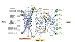
An ML Neural Network (NN) model is proposed to predict the transformation temperatures (TTs) of NiTiHf for a given combination of elemental composition and processing parameters within an acceptable confidence interval. The main challenge in NiTiHf TTs prediction is the high dimensional dependency of TTs to various parameters as well as not fully clear governing physics. Considerable experimental research was performed from 1995 to design the NiTiHf TTs which in turn paved the path to feed the ML algorithms which are now presenting an excellent approach for material design.


A thorough data set is constructed from both unpublished data and available literature and then analyzed to select twenty input parameters to feed the NN model. To model and forecast the TTs of NiTiHf with a wide range of TTs up to 800°C, a total of 173 data points are gathered, verified, and selected. The model’s overall determination factor (R2 )was 0.92, indicating the viability of the proposed NN model in showing the link between material composition, processing factors, and then defining the TTs of NiTiHf alloy. The effort additionally validates the generated results against existing data in the literature. The validation confirms the significance of the proposed model.


Electronic material that grows tougher on impact

Accidents happen every day, and if you drop your smartwatch, or it gets hit really hard, the device probably won’t work anymore. But now, researchers report on a soft, flexible material with “adaptive durability,” meaning it gets stronger when hit or stretched. The material also conducts electricity, making it ideal for the next generation of wearables or personalized medical sensors.

Inspiration for the new material came from a mixture commonly used in cooking — a cornstarch slurry.

“When I stir cornstarch and water slowly, the spoon moves easily,” explains Yue (Jessica) Wang, a materials scientist and the project’s principal investigator. “But if I lift the spoon out and then stab the mixture, the spoon doesn’t go back in. It’s like stabbing a hard surface.” This slurry, which helps thicken stews and sauces, has adaptive durability, shifting from malleable to strong, depending on the force applied. Wang’s team set out to mimic this property in a solid conductive material.

Many materials, such as metals, that conduct electricity are hard, stiff, or brittle. But researchers have developed ways to make soft and bendable versions using conjugated polymers — long, spaghetti-like molecules that are conductive. Yet, most flexible polymers break apart if they undergo repeated, rapid or large impacts. So, Wang’s team at the University of California, Merced, set out to select the right combination of conjugated polymers to create a durable material that would mimic the adaptive behavior of cornstarch particles in water.

Initially, the researchers made an aqueous solution of four polymers: long, spaghetti-like poly(2-acrylamido-2-methylpropanesulfonic acid), shorter polyaniline molecules and a highly conductive combination known as poly(3,4-ethylenedioxythiophene) polystyrene sulfonate (PEDOT:PSS). After spreading a thin layer of the mixture and drying it to make a film, the team tested the stretchy material’s mechanical properties.

They found that rather than breaking apart from very rapid impacts, it deformed or stretched out. The faster the impact, the more stretchy and tough the film became. And surprisingly, just a 10% addition of PEDOT:PSS improved both the material’s conductivity and adaptive durability. Wang notes that this result was unexpected because, on their own, PEDOT and PSS don’t get tougher with rapid or high impacts.

The four polymers, two with positive charges and two with negative charges, tangle up like a big bowl of spaghetti and meatballs, explains Di Wu, a postdoctoral researcher in Wang’s lab who is presenting the work at the meeting. “Because the positively charged molecules don’t like water, they aggregate into meatball-like microstructures,” says Wu. The team’s hypothesis is that the adaptive behavior comes from the meatballs absorbing the energy of an impact and flattening when hit, but not completely splitting apart.

However, Wu wanted to see how adding small molecules could create a composite material that was even tougher when stretched or dropped quickly. Because all the polymers had charges, the team chose molecules with positive, negative or neutral charges to test. Then they assessed how the additives modified the polymers’ interactions and impacted each material’s adaptive durability.

Preliminary results have indicated that the positively charged nanoparticles made of 1,3-propanediamine were the best additive, imparting the most adaptive functionality. Wu says this additive weakened the interactions of the polymers that form the “meatballs,” making them easier to push apart and deform when hit, and strengthened the tightly entangled “spaghetti strings.” “Adding the positively charged molecules to our material made it even stronger at higher stretch rates,” says Wu.

In the future, Wang says, the team will shift toward demonstrating the applicability of their lightweight conductive material. The possibilities include soft wearables, such as integrated bands and backside sensors for smartwatches, and flexible electronics for health monitoring, such as cardiovascular sensors or continuous glucose monitors. Additionally, the team formulated a previous version of the adaptive material for 3D printing and produced a replica of a team member’s hand, demonstrating the potential incorporation into personalized electronic prosthetics. Wang thinks the new composite version should also be compatible with 3D printing to make whatever shape is desired.

The adaptive durability of the material means that future biosensor devices could be flexible enough for regular, human motion but resist damage if they’re accidentally bumped or hit hard, explains Wang. “There are a number of potential applications, and we’re excited to see where this new, unconventional property will take us.”

For more information: ACS

A mutual inductance level sensor system for liquid metals

In the Mechanisms Engineering Test Loop (METL) at the U.S. Department of Energy’s (DOE) Argonne National Laboratory, component and instrument technology for liquid metal fast reactors is tested in sodium at temperatures up to 650°C. This high temperature, along with the reactivity of the sodium, requires unique solutions to simple measurements. One example is monitoring the liquid level in such a system. The ability to do so is very important to the nuclear industry, which is interested in designing sensor systems for use in advanced nuclear reactors. Improvements in this area could lead to more efficient reactors, more economical maintenance and operation of nuclear power plants, and faster commercialization of new designs.

Recently, scientists at Argonne developed a prototype mutual inductance level sensor (MILS), which can accurately and reliably make fluid-level measurements of liquid metals at high temperatures. The sensor utilizes electromagnetism and the electrically conductive nature of the liquid metal to provide continuous level measurements without having to come into contact with the liquid itself.

“The MILS system’s capability to read any electrically conductive working fluid at high temperatures provides new opportunities for operation in industries such as power generation and metallurgy,” said Teddy Kent, principal nuclear engineer at Argonne and lead author. ​“It’s possible for companies to optimize the MILS system, tailoring it to whatever environmental needs are necessary.”

Experimental data collected with the MILS at METL was used to validate a finite element analysis model in ANSYS Maxwell software that can be used to optimize sensor performance. Analysis results indicate the MILS will work effectively with liquid sodium and liquid lead coolants up to 650°C. Additionally, the operating frequency can be optimized for the material and geometry of the sensor and operating environment, and the sensor geometry can be selected to maximize signal sensitivity. The MILS system has been deemed accurate and reliable, and researchers will continue to improve the accuracy of calibration and temperature dependence of the sensor.

For more information: Argonne National Laboratory

Rice researchers develop 3D-printed wood from its own natural components

Researchers at Rice University have unlocked the potential to use 3D printing to make sustainable wood structures, offering a greener alternative to traditional manufacturing methods.

Wood has historically been marred by wasteful practices generated during shaping processes, driving up costs and environmental impact. Now researchers in materials science and nanoengineering at Rice have developed an additive-free, water-based ink made of lignin and cellulose, the fundamental building blocks of wood. The ink can be used to produce architecturally intricate wood structures via a 3D printing technique known as direct ink writing.

“The ability to create a wood structure directly from its own natural components sets the stage for a more eco-friendly and innovative future,” said Muhammad Rahman, an assistant research professor of materials science and nanoengineering at Rice. “It heralds a new era of sustainable 3D-printed wood construction.”

The implications are far-reaching, potentially revolutionizing industries such as furniture and construction.

“Unlike previous attempts, this method exclusively uses nanoscale wood components for 3D printing, marking a significant advancement in the field,” said Pulickel Ajayan, the Benjamin M. and Mary Greenwood Anderson Professor in Engineering and professor and chair of materials science and nanoengineering.

The university’s research focused on optimizing the composition of the ink by adjusting the ratio of lignin, cellulose nanofibers and nanocrystals while maintaining the natural lignin-cellulose balance, according to both M.S.H Thakur and Chen Shi, lead co-authors on the study.

Although lignin is one of the most abundant biopolymers on Earth, it is the least-valued product in industries, noted Amit Naskar, a project collaborator and senior research and development staff at Oak Ridge National Laboratory.

Post-printing, comprehensive analyses were conducted to assess the surface and internal structures of the 3D printed wood, comparing it to natural wood counterparts. The payoff not only exhibited close similarities to natural wood in texture but also in scent and strength.

Additionally, mechanical tests were performed to evaluate compressive and bending strengths, revealing promising results that surpassed those of natural balsa wood.

For more information: Science Advances

Image: Muhammad Rahman (center), an assistant research professor of materials science and nanoengineering at Rice and his lab. Photo courtesy of Gustavo Raskosky/Rice University. 

Scientists reveal the first unconventional superconductor that can be found in mineral form in nature

Scientists from Ames National Laboratory have identified the first unconventional superconductor with a chemical composition also found in nature. Miassite is one of only four minerals found in nature that act as a superconductor when grown in the lab. The team’s investigation of miassite revealed that it is an unconventional superconductor with properties similar to high-temperature superconductors. Their findings further scientists’ understanding of this type of superconductivity, which could lead to more sustainable and economical superconductor-based technology in the future.

Superconductivity is when a material can conduct electricity without energy loss. Superconductors have applications including medical MRI machines, power cables, and quantum computers. Conventional superconductors are well understood but have low critical temperatures. The critical temperature is the highest temperature at which a material acts as a superconductor.

In the 1980s, scientists discovered unconventional superconductors, many of which have much higher critical temperatures. According to Ruslan Prozorov, a scientist at Ames Lab, all these materials are grown in the lab. This fact has led to the general belief that unconventional superconductivity is not a natural phenomenon.

Prozorov explained that it is difficult to find superconductors in nature because most superconducting elements and compounds are metals and tend to react with other elements, like oxygen. He said that miassite (Rh17S15) is an interesting mineral for several reasons, one of which is its complex chemical formula. “Intuitively, you think that this is something which is produced deliberately during a focused search, and it cannot possibly exist in nature,” said Prozorov, “But it turns out it does.”

Paul Canfield, Distinguished Professor of Physics and Astronomy at Iowa State University and a scientist at Ames Lab, has expertise in the design, discovery, growth, and characterization of novel crystalline materials. He synthesized high-quality miassite crystals for this project. “Although miassite is a mineral that was discovered near the Miass River in Chelyabinsk Oblast, Russia,” said Canfield, “it is a rare one that generally does not grow as well-formed crystals.”

Growing the miassite crystals was part of a larger effort to discover compounds that combine very high melting elements (like Rh) and volatile elements (like S). “Contrary to the nature of the pure elements, we have been mastering the use of mixtures of these elements that allow for low-temperature growth of crystals with minimal vapor pressure,” said Canfield. “It’s like finding a hidden fishing hole that is full of big fat fish. In the Rh-S system, we discovered three new superconductors. And, through Ruslan’s detailed measurements, we discovered that the miassite is an unconventional superconductor.”

Prozorov’s group specializes in advanced techniques to study superconductors at low temperatures. He said the material needed to be as cold as 50 millikelvins, which is about -460 degrees Fahrenheit.

Prozorov’s team used three different tests to determine the nature of miassite’s superconductivity. The main test is called the “London penetration depth.” It determines how far a weak magnetic field can penetrate the superconductor bulk from the surface. In a conventional superconductor, this length is basically constant at low temperatures. However, in unconventional superconductors, it varies linearly with the temperature. This test showed that miassite behaves as an unconventional superconductor.

Another test the team performed was introducing defects into the material. Prozorov said that this test is a signature technique his team has employed over the past decade. It involves bombarding the material with high-energy electrons. This process knocks out ions from their positions, thus creating defects in the crystal structure. This disorder can cause changes in the material’s critical temperature.

Conventional superconductors are not sensitive to non-magnetic disorders, so this test would show no or very little change in the critical temperature. Unconventional superconductors have a high sensitivity to disorder, and introducing defects changes or suppresses the critical temperature. It also affects the critical magnetic field of the material. In miassite, the team found that both the critical temperature and the critical magnetic field behaved as predicted in unconventional superconductors.

Investigating unconventional superconductors improves scientists understanding of how they work. Prozorov explained that this is important because, “Uncovering the mechanisms behind unconventional superconductivity is key to economically sound applications of superconductors.”

For more information: Communications Materials

Image: A miassite crystal grown by Paul Canfield.

A new world of 2D material is opening up

Materials that are incredibly thin, only a few atoms thick, exhibit unique properties that make them appealing for energy storage, catalysis and water purification. Researchers at Linköping University have now developed a method that enables the synthesis of hundreds of new 2D materials.

Since the discovery of graphene, the field of research in extremely thin materials, so-called 2D materials, has increased exponentially. The reason is that 2D materials have a large surface area in relation to their volume or weight. This gives rise to a range of physical phenomena and distinctive properties, such as good conductivity, high strength or heat resistance, making 2D materials of interest both within fundamental research and applications.

“In a film that’s only a millimetre thin, there can be millions of layers of the material. Between the layers there can be a lot of chemical reactions and thanks to this, 2D materials can be used for energy storage or for generating fuels, for example,” says Johanna Rosén, professor in Materials physics at Linköping University.

The largest family of 2D materials is called MXenes. MXenes are created from a three-dimensional parent material called a MAX phase. It consists of three different elements: M is a transition metal, A is an (A-group) element, and X is carbon or nitrogen. By removing the A element with acids (exfoliation), a two-dimensional material is created. Until now, MXenes has been the only material family created in this way.

The Linköping researchers have introduced a theoretical method for predicting other three-dimensional materials that may be suitable for conversion into 2D materials. They have also proved that the theoretical model is consistent with reality.

To succeed, the researchers used a three-step process. In the first step, they developed a theoretical model to predict which parent materials would be suitable. Using large-scale calculations at the National Supercomputer Centre, the researchers were able to identify 119 promising 3D materials from a database and a selection consisting of 66,643 materials.

The next step was to try to create the material in the lab.

“Out of 119 possible materials, we studied which ones had the chemical stability required and which materials were the best candidates. First, we had to synthesise the 3D material, which was a challenge in itself. Finally, we had a high-quality sample where we could exfoliate and etch away a specific atom layers using hydrofluoric acid,” says Jie Zhou, assistant professor at the Department of Physics, Chemistry and Biology.

The researchers removed yttrium (Y) from the parent material YRu2Si2, which resulted in the formation of two-dimensional Ru2SixOy.

But to confirm success in the lab, verification is necessary – step three. The researchers used the scanning transmission electron microscope Arwen at Linköping University. It can examine materials and their structures down at the atomic level. In Arwen it is also possible to investigate which atoms a material is made up of using spectroscopy.
“We were able to confirm that our theoretical model worked well, and that the resulting material consisted of the correct atoms. After exfoliation, images of the material resembled the pages of a book. It’s amazing that the theory could be put into practice, thereby expanding the concept of chemical exfoliation to more materials families than MXenes,” says Jonas Björk, associate professor at the division of Materials design.

The researchers’ discovery means that many more 2D materials with unique properties are within reach. These, in turn, can lay the foundation for a plethora of technological applications. The next step for the researchers is to explore more potential precursor materials and scale up the experiments. Johanna Rosén believes that future applications are almost endless.

“In general, 2D materials have shown great potential for an enormous number of applications. You can imagine capturing carbon dioxide or purifying water, for example. Now it’s about scaling up the synthesis and doing it in a sustainable way,” says Johanna Rosén.

For more information: Science

Image: In the electron microscope Arwen materials can be studied at an atomic level.

LLNL scientists advance light-responsive material

Researchers at Lawrence Livermore National Laboratory, Livermore, Calif., have furthered a new type of soft material that can change shape in response to light, a discovery that could advance “soft machines” for a variety of fields, from robotics to medicine.

Continue reading

Penguins, Covestro and Carnegie Mellon partner for seventh annual ‘Rethink the Rink’ Make-A-Thon

The Pittsburgh Penguins are teaming up once again with international giants of science and technology, Carnegie Mellon University (CMU) and Covestro, the official innovation partner of the Penguins. This marks the seventh annual “Rethink the Rink,” a continuing showcase of innovation and ingenuity to make hockey safer at every level, from youth hockey to the NHL.

The signature event will encourage CMU students to use Covestro’s leading-edge material technologies to develop innovative prototypes of hockey equipment at the University’s makerspace, TechSpark. The event will culminate in a series of prototype pitches to a panel of judges with expertise in professional hockey, advanced materials and hockey equipment, with the best prototypes potentially continuing development and becoming commercially available.

This year’s Rethink the Rink Make-A-Thon is focused on an important safety measure in hockey- neck protection equipment to protect a player’s neck from skate blades. Following the tragic passing of former Penguin Adam Johnson in October 2023, more hockey teams and leagues are instilling mandates that players utilize neck protection on the ice.

Sixteen CMU students will have one week to ideate solutions, develop and test prototypes, and create a compelling presentation to explain their concepts to a panel of expert judges from the Penguins, Covestro, Bauer Hockey and CMU’s College of Engineering. To help them achieve their goal, the students will have help from coaches, including materials experts from Covestro and hockey professionals from the Penguins.

“Safety is central to the work we do at Covestro,” said Samir Hifri, Covestro LLC chairman and president. “Combining safety with another of Covestro’s core strengths, innovation, to create an environment where the best and the brightest student minds can leverage insights from experts in hockey and material science is a win-win for all the organizations involved and the sport of hockey.”

The “Rethink the Rink” partnership began in 2017 when the Penguins, Covestro, and CMU joined forces to bolster player safety and foster a sustained pipeline of hockey innovation.

For more information: NHL.com

Redefining material science: Scientists have induced polarity in metals

In the field of materials science, the concepts of polarization and polarity are typically linked to insulators. Imagine, though, if we could introduce these properties into metals. This could reduce the power losses associated with semiconductors and enhance the longevity of batteries used in electronic devices. Up to now, despite intensive academic research aimed at inducing polarization and polarity in metals, current technologies have faced significant challenges.

Recent breakthrough by the collaborative efforts of Professor Daesu Lee from the Department of Physics at Pohang University of Science and Technology (POSTECH), Professor Tae Won Noh and Dr. Wei Peng from the Department of Physics and Astronomy at Seoul National University (SNU), and Professor Se Young Park from the Department of Physics at Soongsil University (SSU), have led to the discovery of a method to induce and control polarization and polarity states within metals.

Free electrons within metals, given their name, exhibit unrestricted movement, making it difficult to align them in specific directions to induce polarization or polarity states. Additionally, the symmetric structure of metal crystals at both ends has historically posed challenges in inducing these electrical effects.

However, the research team employed flexoelectric fields to implement polarization and polarity states within metals. This type of field arises when the surface of an object undergoes non-uniform deformation, allowing for the manipulation of charge movement and electrical characteristics by subtly altering the lattice structure of metals.

The team applied external pressure to the widely used strontium ruthenate (SrRuO3) in the field of electronic components and semiconductors, generating a flexoelectric field. This metal oxide, characterized by heteroepitaxy, where crystals of strontium and ruthenium oxide with different shapes grow in the same direction, possesses a centrosymmetric structure.

The flexoelectric field altered the electronic interactions and lattice structure within strontium ruthenate, leading to a successful induction of polarization within the metal, causing a transformation in its electrical and mechanical properties and breaking the previously central symmetric structure. By employing flexoelectric polarizing and control of a ferromagnetic metal, the research team has successfully unraveled the mystery surrounding the implementation of polarization and polarity within metallic substances.

The study’s lead researcher, Professor Daesu Lee from POSTECH, stressed, “We are the first researchers to verify the universal implementation of polarity states within metallic substances. I am hopeful that the findings from this study will prove beneficial in crafting highly efficient devices within the semiconductor and electrical fields.”

For more information: Nature Physics

Bio-inspired materials showcase potential for protective equipment and textiles

Bio-inspired materials (BIM) are synthetic materials whose structure and properties are similar to natural materials or living matter. These materials have the potential to advance structural materials, textiles and protective equipment due to their durability and self-healing properties.

Dr. Vanessa Restrepo, assistant professor in the J. Mike Walker ’66 Department of Mechanical Engineering, and her team at the Bio-Inspired Materials (BIM) Lab aim to create bio-inspired materials with enhanced behaviors by focusing on the nature of proteins to develop the sacrificial bond composites (bonds that break before the main structural link is broken) utilizing non-linear adhesive materials.

This research could significantly impact electrical wired infrastructure in adverse weather conditions. Using these materials, the cables could stretch and extend to bear the additional weight of ice accumulation or sudden tree falls caused by strong winds. This flexibility could prevent cable breakage, meaning less interruptions in electrical service.

“Our commitment remains dedicated to advancing bioinspired materials and their applications in various industries,” said Restrepo. “We’re enthusiastic about these materials’ potential impact and contribution to more resilient and sustainable product development.”

According to Restrepo, non-linear adhesives refer to a force-displacement behavior that deviates from a bilinear path, in contrast to conventional adhesives. Unlike traditional adhesives, the force-displacement relationship of non-linear adhesives does not follow a straightforward, two-stage pattern. Instead, it exhibits a more complex and variable behavior as external forces are applied.

To approach this research, Restrepo is using a cross-scale strategy, integrating non-linear adhesive materials and opposite-facing magnets to form sacrificial bond composites similar to those found in proteins such as the nacre’s interface, which is a multilayered brick-and-mortar natural material 3000 times more resistant to fracture than its constituents.

Their approach involves utilizing sacrificial bond composites that mimic natural biological mechanisms, allowing for energy dissipation and self-healing upon mechanical failure. The external load breaks the sacrificial bonds of sacrificial bond composites, and the opposite-facing magnets bring together the separated interface, allowing the reforming of its sacrificial bonds and the self-repairing of the composite after sustaining large strains.

“This differs significantly from current materials that lack these intrinsic self-repairing abilities, resulting in single-use and disposable products,” she said. “Our proposed research looks at the possibility of creating multiuse self-repairing energy dissipation mechanisms, such as Fall Arresters.”

Incorporating these innovative materials could result in longer-lasting, more cost-effective, and more sustainable products that require less frequent replacement, eventually resulting in the development of self-repairing materials used in various everyday items, such as protective equipment and textiles.

The BIM lab partnered with Dr. Ramses Martinez, associate professor at Purdue University, to conduct this research. This method was recently patented by Restrepo and team.

For more information: Materials & Design

Image: Dr. Vanessa Restrepo showcases prototype of bio-inspired materials. Credit: Texas A&M Engineering

Molecular tape promises seamless transfer and scale up of 2D materials

Materials so thin they are considered two-dimensional are only a couple atoms thick and, at this scale, they behave in surprising ways. Graphene, for example, is ultrathin graphite, the same material used in pencils. But once sliced to a nanosized thickness, it becomes stronger than steel by weight and is among the best materials for conducting electricity.

As with graphene and many other 2D materials, the same attribute that makes them so attractive — their thickness — is also holding back large-scale production. That’s because 2D materials are fragile and prone to damage when researchers attempt to move them or use them in a device.

To overcome this and unlock 2D materials’ potential for commercial production, researchers have recently developed a “molecular tape” that gently adheres to ultrathin materials and selectively releases them exactly where needed using only UV light.

“The variety of 2D materials has vastly increased since the isolation of graphene in 2004, with materials covering the whole range of electronic and magnetic properties,” explained Hiroki Ago, professor at Kyushu University and lead author of the study.

Ago’s lab has spent 10 years developing synthesis techniques for a variety of 2D materials, like high-quality graphene and metal 2D semiconductors. “Many researchers requested our samples, but most of them had problems transferring these 2D materials to their substrates,” he explained. “Due to the thin and delicate nature of 2D materials it is very difficult to transfer them for scientific research and industrial applications,” he said, meaning many promising materials are stuck in the labs where they are produced.

“Therefore, I thought if they can easily transfer 2D materials onto their specific substrates by themselves, 2D materials research and applications will be strongly boosted,” said Ago.

To make the tape user-friendly and simple, Ago and his colleagues devised a material that could selectively stick and un-stick to the 2D materials using UV light. This reduces the chance for damage to occur when the 2D materials are transferred from one surface and to another.

The base of the new tape is a thin layer made from a plastic polymer which gives the tape enough rigidity to be stable and enough flexibility to not damage the materials during transport. Next comes a special blend of polymers — long, chain-like structures made from repeating molecules — that safely attaches to the 2D materials.

“When first adhered to the 2D material, the adhesive layer is soft enough, enabling a uniform contact with the surface and facilitating a full transfer,” Ago said.

Within this adhesive blend, however, are some UV-sensitive polymers which, when exposed to UV light, crosslink, meaning they form a series of repeating, tight bonds throughout the polymer, hardening the adhesive layer. As the tape hardens, it cleanly detaches from and releases the 2D material without the need for destructive manual or chemical processing to remove the tape.

By manipulating the composition of the polymers in the adhesive, the team could fine-tune stickiness and release of the tape for a variety of different 2D materials. “This adaptability ensures the versatility of the UV tapes and their potential in a broad range of applications,” Ago said.

Tests showed the tape greatly reduced the amount of residue and cleaning required after transfer and produced more uniform transfers with fewer cracks when compared to standard methods. “And it allowed for the transfer of larger areas up to the size of 4-inch wafers, which is essential for the adoption of 2D materials at industrial scales,” Ago said.

The tape surprised everyone though when the team tested scenarios beyond their initial designs. It proved successful when transferring 2D materials to fragile or curved surfaces, and the team was able to precisely layer different 2D materials together. Mixing and matching layers and controlling the angles between them, known as twist angles, can significantly boost electrical properties, leading to superconductive states for example.

The team also showed that they could easily cut the tape and transfer different shapes and sizes, enabling researchers to selectively transfer and position custom-sized 2D sheets quite easily. This ability to customize should reduce the amount of adhesive needed and further lower production costs for industry.

The team is now working to improve the composition of the adhesive layer as there is still some wrinkling and bubbling occurring. Efforts are also being made to scale up the sizes, and to one day transfer patterned 2D materials.

For more information: Nature Electronics

Researchers capture strange behavior of laser-excited gold

New research, conducted at the Department of Energy’s SLAC National Accelerator Laboratory, illuminates the strange behavior of gold when zapped with high-energy laser pulses.

When certain materials, such as silicon, are subjected to intense laser excitation, they quickly fall apart. But gold does the opposite: It becomes tougher and more resilient. This is because the way the gold atoms vibrate together—their phonon behavior—changes.

“Our findings challenge previous understandings by showing that, under certain conditions, metals like gold can become stronger rather than melting when subjected to intense laser pulses,” said Adrien Descamps, a researcher at Queen’s University Belfast who led the research while he was a graduate student at Stanford and SLAC. “This contrasts with semiconductors, which become unstable and melt.”

For decades, simulations hinted at the possibility of this phenomenon, known as phonon hardening. Now, using SLAC’s Linac Coherent Light Source (LCLS), the researchers have finally brought this phonon hardening to light.

“It’s been a fascinating journey to see our theoretical predictions confirmed experimentally,” said collaborator Emma McBride, a researcher at Queen’s University Belfast who was previously a Panofsky fellow at SLAC’s High Energy Density Science (HEDS) division. “The precision with which we can now measure these phenomena at LCLS is astonishing, and it opens up new possibilities for future research in material science.”

In their experiment, the team targeted thin gold films with optical laser pulses at the Matter in Extreme Conditions experimental hutch, then used super-fast X-ray pulses from LCLS to take atomic-level snapshots of how the material responded. This high-resolution glimpse into the atomic world of gold allowed researchers to observe subtle changes and capture the moment when its phonon energies increased, providing concrete evidence of phonon hardening.

“We used X-ray diffraction at LCLS to measure the structural response of gold to laser excitation,” McBride said. “This revealed insights into the atomic arrangements and stability under extreme conditions.”

The researchers found that when gold absorbs extremely high-energy optical laser pulses, the forces holding its atoms together become stronger. This change makes the atoms vibrate faster, which can change how the gold responds to heat and might even affect the temperature at which it melts.

“This work resolves a long-standing question about the ultrafast excitation of metals and shows that intense lasers can completely alternate the response of the lattice,” said Siegfried Glenzer, director of the High Energy Density Division at SLAC.

Researchers believe similar phenomena could exist in other metals such as aluminum, copper, and platinum. Further exploration could lead to a better understanding of how metals behave under extreme conditions, which will aid in the development of more resilient materials.

“Looking ahead, we’re excited about the potential to apply these findings to more practical applications, such as in laser machining and material manufacturing, where understanding these processes at the atomic level could lead to improved techniques and materials,” Descamps said. “We’re also planning more experiments and hoping to explore these phenomena across a wider range of materials. It’s an exciting time for our field, and we’re looking forward to seeing where these discoveries take us.”

For more information: Science Advances

Image: Schematic of the experimental setup used to measure the temporal evolution of the diffraction pattern from laser-heated, free-standing Au foils at the LCLS. A transmission image of the nearly Gaussian transform-limited optical laser pulse is shown in the bottom left inset along with a set of contours corresponding to the best 2D Gaussian fit to the data. Azimuthally integrated diffraction patterns at different time delays are shown in the top right inset. Credit: Science Advances (2024).

Pioneering aluminum-magnesium laminates set to transform aerospace and automotive industries

Magnesium alloys, known for their lightweight and high strength, face limitations due to poor corrosion resistance. The innovative Al/Mg/Al laminates combine the benefits of magnesium alloy and aluminum, offering a solution with enhanced mechanical properties and corrosion resistance, critical for aerospace, automotive, and electronic applications.

Magnesium alloys are prized in aerospace, automotive, and electronics for their lightness and strength but are limited by poor corrosion resistance. To overcome this, researchers have developed Al/Mg/Al laminates, cladding magnesium with aluminum to combine their strengths: lightweight with better corrosion resistance. Various methods like co-extrusion, casting, and welding have been explored, with rolling emerging as a preferred technique for its flexibility and efficiency.

The study developed Al/Mg/Al laminates with large thickness ratios, presenting significant advancements in mechanical properties and interfacial bonding strength.

The team from Taiyuan University of Technology has discussed the development and analysis of Al/Mg/Al laminates with varied initial thickness ratios (ITR) created through a hot-rolling process. By experimenting with ITRs ranging from 5 to 40, the study explored how changing the ITR affects the stress, strain, microstructure evolution, and overall properties of the laminates. Findings indicated that an optimal ITR exists—specifically, an ITR of 20—where the laminates exhibit the best comprehensive mechanical properties. This includes maximizing the ultimate tensile strength and yield strength while also achieving high interfacial bonding strength and optimal elongation. Beyond this optimal point, increases in ITR lead to a decrease in interface bonding strength, affecting the laminate’s overall performance. This research contributes to the understanding of how to manipulate laminate composition for enhanced structural applications, particularly in industries seeking lightweight yet strong materials.

Lead researcher, Tao Wang, emphasizes, “Al/Mg/Al laminates with large thickness ratios not only fully utilize the lightweight advantages of magnesium alloys, but also significantly optimize the laminate’s mechanical properties and corrosion resistance, marking a significant step towards the practical application of these materials in advanced engineering fields.”

This breakthrough hints at a transformative future for aerospace and automotive industries, promising materials that are lighter, stronger, and more corrosion-resistant, setting a new standard in composite material development with wide-reaching industrial implications.

For more information: Transactions of Nonferrous Metals Society of China

Image: Schematic diagram of large thickness ratio Al/Mg/Al laminate rolling process.